BGA (Ball Grid Array) has many different types, each with distinct characteristics and suitable applications. The choice of BGA depends not only on the type of product you wish to manufacture but also on various factors such as overall production cost, the final product's weight, product quality, heat generation, and more.
Ceramic Ball Grid Array (CBGA) uses a ceramic substrate to achieve higher thermal stability and mechanical stability, making it very suitable for high-reliability applications. In CBGA, the ratio of tin to lead is 10:90. Due to its extremely high melting point, CBGA requires the C4 method (Controlled Collapse Chip Connection) to bridge the BGA and PCB. CBGA is usually more expensive than PBGA and is suitable for high-performance computing devices, the telecommunications industry, and other similar applications.】
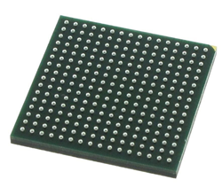
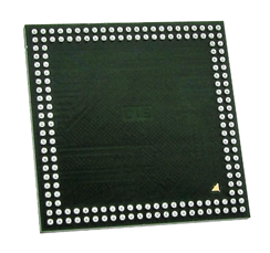
PBGA, short for Plastic Ball Grid Array, is a BGA package that uses a plastic laminate substrate and is one of the most common BGA types in use today. PBGA uses bismaleimide triazine (BT) resin as a substrate material to form a core material, and together with the application of overmolded pad array carrier (OMPAC) sealant technology or ball-to-pad array carrier (GTPAC), it has been proven by JEDEC (Solid State Technology Association) to be highly reliable (Grade 3). This type of BGA typically contains 200 to 500 ball arrays, depending on the application and package size. PBGA is suitable for industries including consumer electronics, communications equipment and low to medium power applications, etc.
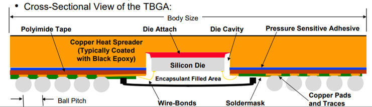
Tape Ball Grid Array (TBGA) is a type of BGA packaging technology that utilizes a flexible tape substrate instead of the traditional rigid laminate. This allows for thinner and lighter packaging with high-density interconnections and improved thermal and electrical performance. TBGA is commonly used in advanced applications such as portable electronic devices and high-performance computing.
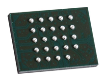
Freescale Semiconductor (Tape Ball Grid Array (TBGA) Overview)
Package on Package (PoP) involves stacking multiple integrated circuits (ICs) together, each with its own BGA, to achieve vertical integration of components. The existence of PoP technology is to meet the continuous demand in the electronics industry for fine pitch, small size, high signal processing speed, and smaller installation space in electronic products such as smartphones and digital cameras. During the PCB assembly process, this technology electrically connects the memory devices in the top package with the logic devices in the bottom package, allowing for separate testing and replacement, which can reduce the cost and complexity of the PCB structure.
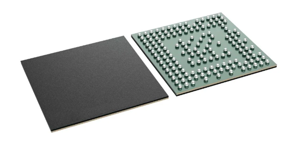
The Flip Chip Ball Grid Array (FCBGA) involves flipping the integrated circuit and directly soldering it onto the PCB, with its solder balls directly connecting to the pads on the printed circuit board (PCB). This design is different from traditional lead frame packaging as it eliminates the leads, thus achieving high-density connections, improved electrical performance, and better thermal management. Compared to other BGA types, its main advantage is shorter electrical paths, resulting in superior conductivity and higher performance speeds. FCBGA is widely used in high-performance computing, graphics processing, networking equipment, communication devices, and other electronic products requiring high density and high speed.