By Hesam Moshiri, Anson Bao
Copyright: Attribution-NonCommercial-NoDerivs (CC-BY-NC-ND)
A DC-to-DC converter is one of the most commonly used circuits in electronics, especially in power supply applications. There are three major types of DC-to-DC converters (non-isolated): Buck, Boost, and Buck-Boost. Sometimes a buck converter is also called a step-down converter and a boost converter is also called a step-up converter.
In this article/video, I introduce an adjustable 5A DC-to-DC converter circuit that uses an advanced chip, made by Texas Instruments, which is TPS5450. It’s a high-frequency and efficient buck converter chip that provides tight voltage regulation. I have followed several PCB design rules to ensure low noise, low EMI, and high stability of the output voltage.
To design the schematic and PCB, I used Altium Designer 23 and shared the project with my friends using Altium-365. The fast component search engine (Octopart) allowed me to quickly consider components’ information and also generate the BOM. To get high-quality fabricated boards, I sent the Gerber files to PCBWay and tested the circuit for output stability and noise, using a DC load, A multimeter, and an oscilloscope. Soon later, I will also perform the step-response test and demonstrate the results.
Download the Gerber or order 10Pcs high-quality boards, for just 5 USD
If you like to order a fully assembled PCB board (including Free Shipping), Just click here
Specifications
Input Voltage: 5.5V to 36V
Output Voltage: 1.22Vmin to 31Vmax (variable)
Output Current (continuous): 5A
Output Current (peak, short time): 6A
Maximum Output Drop: 22mV (5A load)
Output Noise: 14mVp-p (no load), 50mVp-p (5A load), 20MHz-BW
Circuit Analysis
Figure 1 shows the schematic diagram of the device. As it is clear, the heart of the circuit is IC1 [1], which is an advanced buck converter made by Texas Instruments.
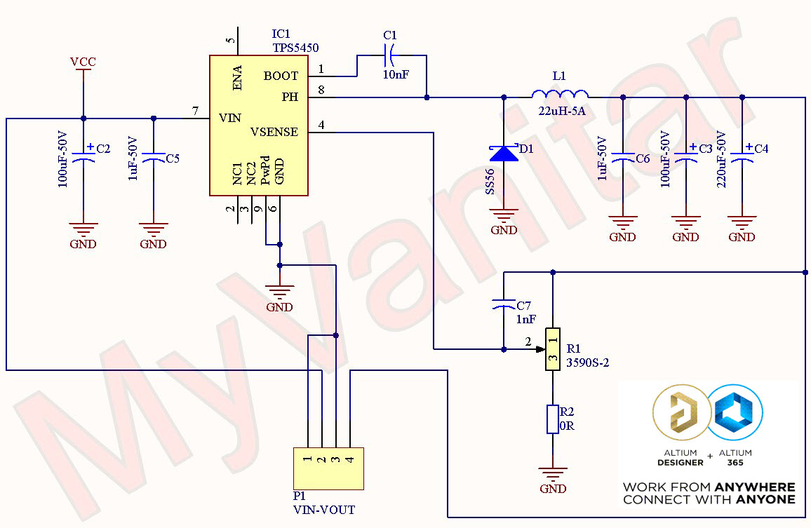
Figure 1
Schematic diagram of the 5A Adjustable Switching Power Supply (Altium)
C2 and C5 and input bypass capacitors. They are critical components. Please watch the YouTube video for PCB designing rules. IC1 is the main component of the circuit. According to the component datasheet: “The TPS5450 is a high-output-current PWM converter that integrates a low-resistance, high-side N-channel MOSFET. Included on the substrate with the listed features are a high-performance voltage error amplifier that provides tight voltage regulation accuracy under transient conditions; an Undervoltage-lockout circuit to prevent start-up until the input voltage reaches 5.5V; an internally set slow-start circuit to limit inrush currents; and a voltage feedforward circuit to improve the transient response. Using the ENA pin, the shutdown supply current is reduced to 18μA typically. Other features include an active-high enable, overcurrent limiting, overvoltage protection, and thermal shutdown. To reduce design complexity and external component count, the TPS5450 feedback loop is internally compensated.”
D1 is the SS56 Schottky diode [2]. D1, L1, and IC1 are the essential elements of a buck converter. C3, C4, and C6 are output capacitors to reduce the noise.
R1 is a 5K potentiometer [3] to adjust the output voltage. If you plan to have full control over the output voltage from 1.2V to 31V, the value of the R2 should be zero (you solder a 0R-0805 resistor), otherwise, if you plan to limit the maximum output voltage, you need to use a resistor there. For example, by using a 5K potentiometer and a 470R resistor for R2, the maximum output voltage would be around 14.5V. Therefore, if you plan to use this power supply for the range of 1.2V to 12V, these values are fine. The advantage of using R2 is that you will have much better control over the voltage range, which means you can adjust the potentiometer more precisely. To get other output voltages, you just need to change the R2 value and find the best value with just a few experiments.
PCB Layout
Figure 2 shows the layout of the design. It’s a two-layer PCB board and it is designed to be as compact as possible. The backside (Bottom layer) of the PCB board is a solid ground plane. Figure 3 shows a 3D view of the PCB board and assembly drawings.
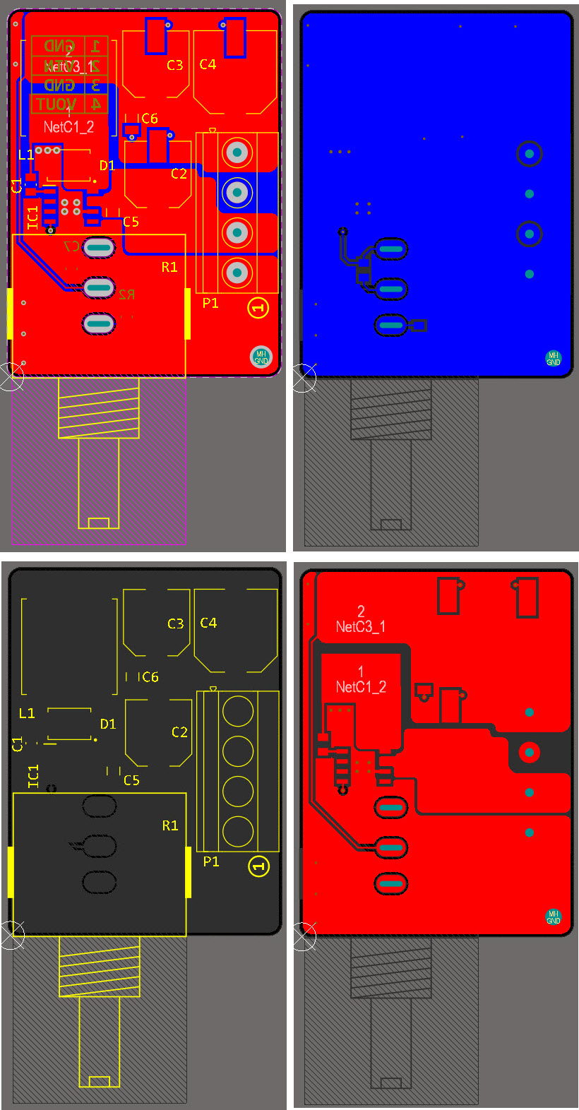
Figure 2
PCB layout of the 5A Adjustable Switching Power supply
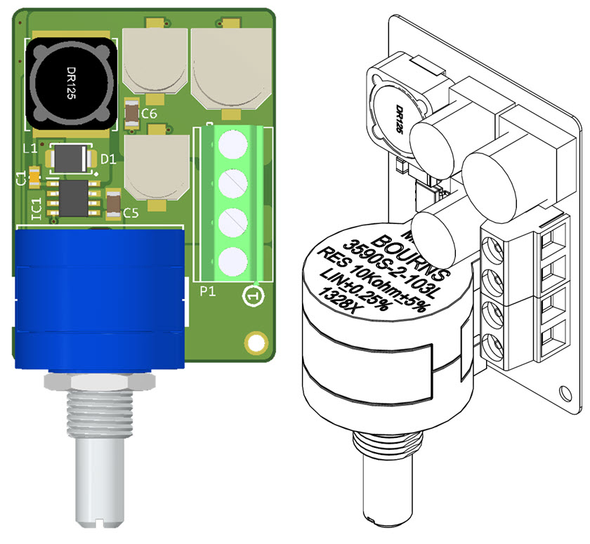
Figure 3
A 3D view of the PCB board and assembly drawings
Test and Verification
There are 3 tests to examine the performance of a buck converter: Line/Load regulation, output noise, and step-response test. Please watch the video for more details. The converter board demonstrated around a 10mV voltage drop only, under a 3A load. Figure 4 shows the output noise with no load at the output and figure 5 shows the output noise by applying a 3A load (using a DC load). This noise can be easily reduced even further just by adding a few decoupling capacitors just as close as possible to the load.
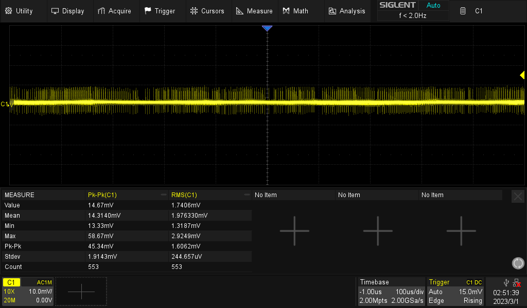
Figure 4
Output noise of the power supply (no load)
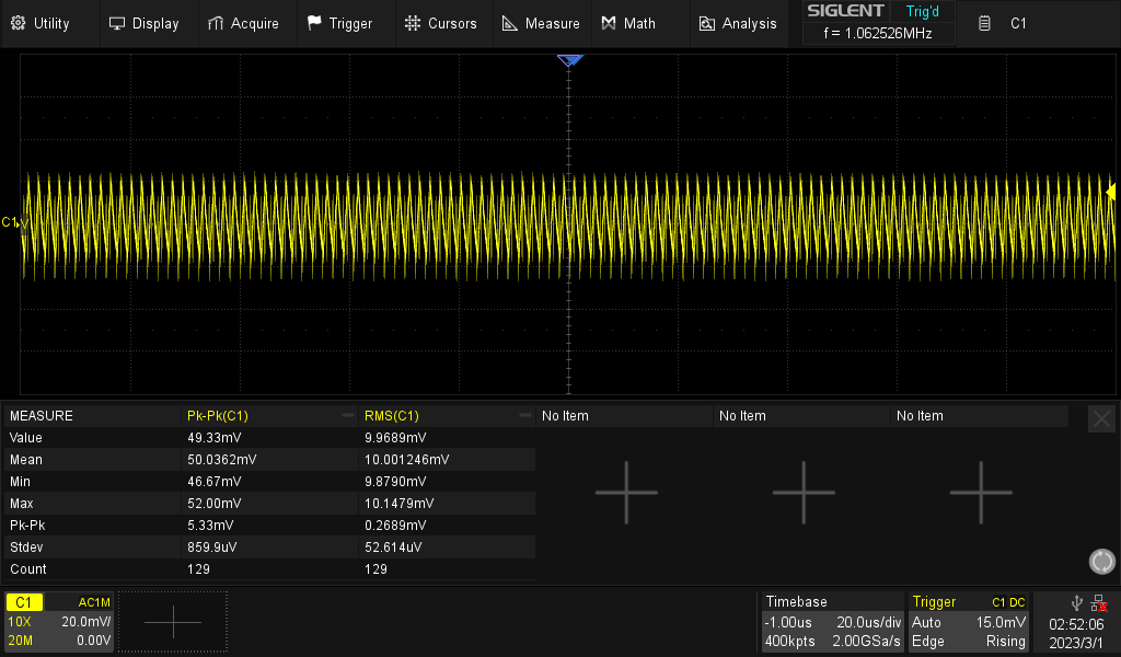
Figure 5
Output noise of the power supply (maximum load, 5A)
Bill of Materials
Figure 6 shows the bill of materials for the project. The Octopart website is not just a fast search engine for electronic components but also a very nice tool to build any kind of BOM for free.
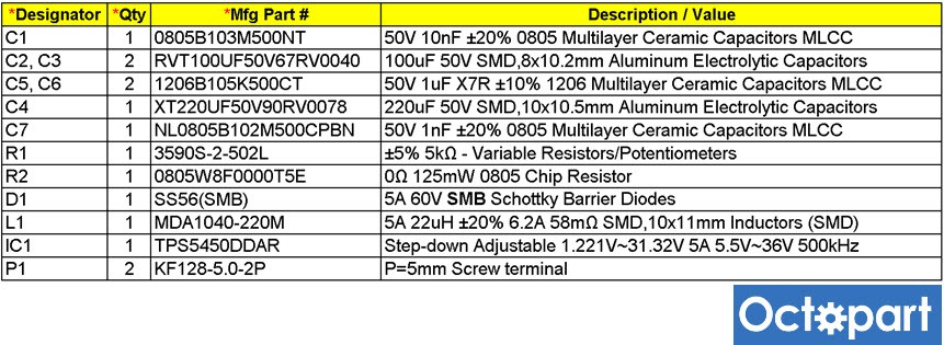
Figure 6
Bill of materials for the 5A-35V Adjustable Switching Power Supply
References
[1]: TPS5450: https://octopart.com/tps5450ddar-texas+instruments-7105511?r=sp
[2]: SS56: https://octopart.com/ss56bf-hf-comchip-107339894?r=sp
[3]: 3590-S2: https://octopart.com/3590s-2-502l-bourns-112621?r=sp


