By Hesam Moshiri, Anson Bao
DC to DC buck converters is a famous topology in the electronic and a widely used circuit in electronic devices. A buck converter steps down the input voltage while it increases the output current. In this article/video, I have discussed a DC to DC buck converter that can be used effectively as a switching power supply. The output voltage and current are adjustable: 1.25V to 30V and 10mA to 6A (continuous). The power supply supports the constant voltage (CV) and constant current (CC) features. Two LEDs demonstrate the CV and CC status. The circuit is compact and both sides of the PCB have been used to mount the components.
To design the schematic and PCB, I used Altium Designer 21, also the SamacSys component libraries (Altium plugin) to install the missing schematic symbols/PCB footprints. To get high-quality fabricated PCB boards, I sent the Gerbers to PCBWay.
To test the circuit, I used the power analysis feature of the Siglent SDS2102X Plus oscilloscope (or SDS1104X-E), Siglent SDL1020X-E DC Load, and Siglent SDM3045X multimeter. Isn’t cool, so let’s get started!
· Download the Gerbers or order 10Pcs high-quality PCBs for just 5.0USD
· To order a fully assembled PCB board (plus FREE shipping). Please contact: anson@pcbway.com
Specifications
A. Circuit Analysis
Figure 1 shows the schematic diagram of the switching power supply (DC to DC buck converter). The schematic diagram contains 3 main parts: the buck converter, feedback loop, and opamp regulator.

Figure 1
schematic diagram of the adjustable switching power supply
PSI is the XL4016 controller chip [1] and the main component of the buck converter. D2 is the MBR20100 Schottky diode [2] and L2 is a 47uH-10A inductor that are other essential components of the buck converter circuit. C3..C9 are used to reduce the input/output noises.
R2 is a 20K multiturn potentiometer (trimmer) that provides a feedback path to the controller chip to adjust the output voltage. C1 is used to reduce the noise on the feedback path. R1 is just a 0R resistor that is used as a jumper on the PCB board. R4 is the shunt resistor that is made of two 0.1R-5W resistors. These two resistors are connected in parallel to make a single 0.05R-10W resistor.
IC2 is the TS4264 linear regulator chip [3] that provides a stable +5V supply rail. C15 is used to reduce the output noise of the regulator.
IC1 is the MCP6002 opamp [4] that is used to amplify the small shunt resistor voltage to provoke the feedback pin of the PS1. D1 provides a feedback path to the PS1. The MCP6002 chip provides two opamps. The first opamp is configured as a non-inverting amplifier and the second opamp is configured as a comparator to feed D3 and D4 LEDs (CC, CC). R5, C11..C13 create a low pass RC filter to reduce the supply noise to IC1. R9 and C14 also build a low pass RC filter to remove the shunt noises. C10 is also used to reduce the amplifier noise.
B. PCB Layout
Figure 2 shows the PCB layout of the variable switching power supply board. It is a two layers PCB board and a mixture of SMD and through-hole components have been used to make it as compact as possible.

Figure 2
PCB layout of the adjustable switching power supply
I used the Altium Designer software [5] to design the schematic and PCB. I did not have the schematic symbols, PCB footprints, and 3D models of several components in this project. So instead of wasting my time in designing the component libraries from scratch and increase the risk of errors and mismatches, I used the free and IPC-rated SamacSys component libraries and imported them right into the Altium PCB project using the SamacSys Altium plugin [6]. SamacSys provides plugins for the majority of electronic designing CAD software [7], not just for the Altium Designer. Figure 3 shows the supported electronic designing CAD software.

Figure 3
SamacSys Supported electronic designing CAD software (plugins)
Specifically, I used the SamacSys libraries for PS1[8], IC1[9], IC2 [10], and D2[11] which you can consider in the references. Another option is to download the component libraries from componentsearchengine.com and import them manually. Figure 4 shows the selected components in the SamacSys Altium plugin.
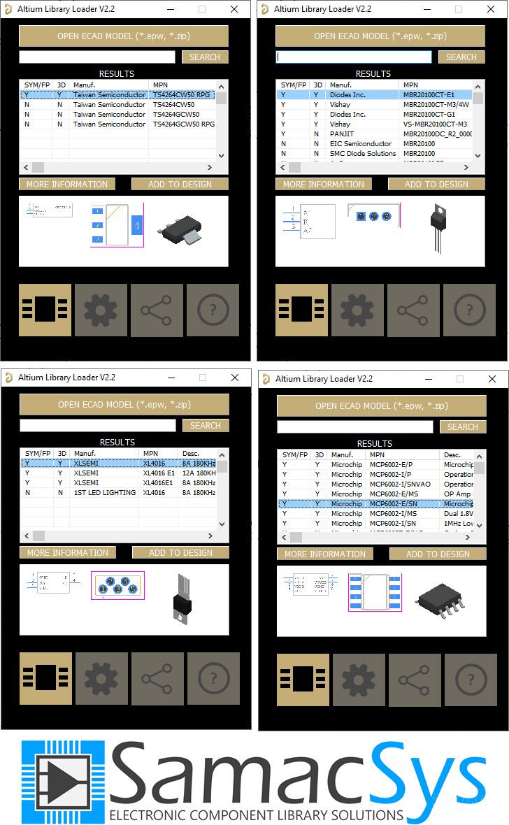
Figure 4
Selected components in the SamacSys Altium plugin
C. Assembly and Test
Figure 5 shows the assembled board from the top and bottom view. As it is clear that both sides of the PCB have been used to mount the components. As you see high-current carrying tracks are partially covered by the solder mask. You must strengthen these tracks using solder and/or copper wires (tinning).

Figure 5
Assembled PCB board (top and bottom view)
C-1. Output Noise
I used the power analysis feature of the Siglent SDS2102X Plus oscilloscope [12] to measure the output noise. Surely you can use the cheaper Siglent SDS1104X-E oscilloscope [13] and replicate the experiment without any problem, however, the plus one is a role model device.
The first test is to check the output noise of the power supply under no load. For this purpose, I should remove the ground lead of the oscilloscope probe, remove the probe’s head, and place a ground spring on the head (figure 6). Also, enable the 20MHz bandwidth limit of the input channel and put the probe on X10.

Figure 6
Preparing the oscilloscope probe to measure the power supply noise
Then put the probe tip directly on the output of the power supply. Figure 7 shows the output noise of the power supply under no load.

Figure 7
The output noise of the adjustable switching power supply
(no load, 20MHz BW limit)
The best choice to build stable and accurate DC loads, is a commercial DC load, such as the Siglent SDL1020X-E [14]. This device guarantees the stability and accuracy of the load in a variety of modes, such as CC, CV, CP, CR .. etc. The CC mode of the SDL1020X-E model is limited to 5A, so let’s test the output noise under a 5A load for now. Figure 8 shows the output noise of the power supply under a 5A load. You can consider the screens of the DC load and the oscilloscope.

Figure 8
The output noise of the adjustable switching power supply
(5A load, CC mode, 20MHz BW limit)
To test the output noise under a 6A load (max continuous), I set the DC load on CR (constat resistance) and changed the value of the resistor to read 6A at the output of the power supply. Figure 9 shows the output noise under a 6A load.
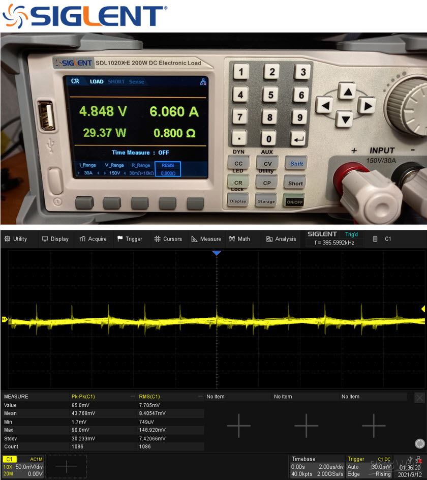
Figure 9
The output of the adjustable switching power supply
(6A load, CR mode, 20MHz BW limit)
Figure 10 shows the output noise of the power supply (6A load), after applying the 16 points averaging using the math function (brown waveform).

Figure 10
The output noise of the adjustable switching power supply
(6A load, CR mode, 20MHz BW limit, 16P averaging)
D. CC Adjustment
There are two methods to adjust the constant current limit of the power supply: using a DC load or using a multimeter [15]. Both methods are quite easy to perform. Just follow the YouTube video.
E. Bill of Materials
Figure 11 shows the bill of materials for the projects. Please consider that I have not included the L1 and the heatsink in the bill of materials for the assembly. Make sure that your selected/built inductor (ferrite core) can tolerate at least 10A (47uH). The hole diameter of the inductor’s pads is 1.3mm.
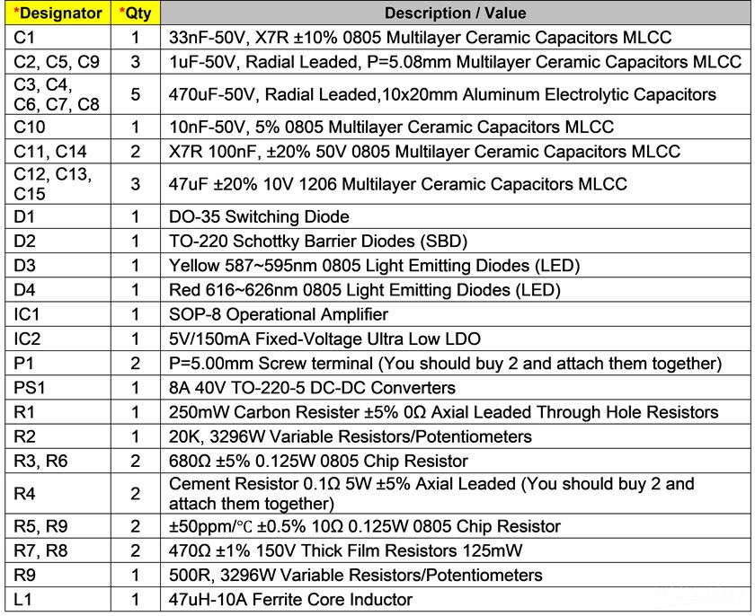
Figure 11
The bill of materials of the adjustable switching power supply
F. References
[1]: XL4016 datasheet: http://www.xlsemi.com/datasheet/xl4016%20datasheet.pdf
[2]: MBR20100 datasheet: https://www.diodes.com/assets/Datasheets/MBR20100C.pdf
[3]: TS4264 datasheet: https://www.mouser.com/datasheet/2/395/TS4264_D15-1142598.pdf
[4]: MCP6002 datasheet: https://componentsearchengine.com/Datasheets/2/MCP6002T-I_SN.pdf
[5]: Altium Designer: https://www.altium.com/yt/myvanitar
[6]: SamacSys Altium plugin: https://www.samacsys.com/altium-designer-library-instructions
[7]: Supported SamacSys plugins: https://www.samacsys.com/pcb-part-libraries
[8]: XL4016 schematic symbol, PCB footprint, 3D model: https://componentsearchengine.com/part-view/XL4016/XLSEMI
[9]: MCP6002 schematic symbol, PCB footprint, 3D model: https://componentsearchengine.com/search?term=mcp6002
[10]: TS4264 schematic symbol, PCB footprint, 3D model: https://componentsearchengine.com/part-view/TS4264CW50%20RPG/Taiwan%20Semiconductor
[11]: MBR20100 schematic symbols, PCb footprint, 3D model: https://componentsearchengine.com/part-view/MBR20100CT-G1/Diodes%20Inc.
[12]: Siglent SDS2102X Plus oscilloscope: https://siglentna.com/digital-oscilloscopes/sds2000xp/
[13]: Siglent SDS1104X-E oscilloscope: https://siglentna.com/digital-oscilloscopes/sds1000x-e-series-super-phosphor-oscilloscopes/
[14]: Siglent SDL2010X-E DC Load: https://siglentna.com/dc-electronic-load/sdl1000x/
[15]: Siglent SDM3045X Multimeter: https://siglentna.com/digital-multimeters/sdm3045x-digital-multimeter/


