 Mila
Sep 07,2026
1759
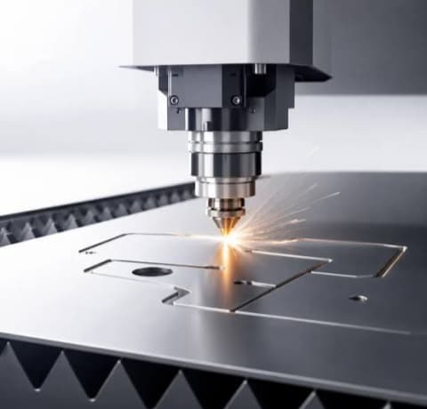
Sheet Metal Cutting Design Guidelines
This guide is designed to help engineers and designers prepare CAD and STEP files that meet manufacturing standards. Following these design requirements prior to order submission helps prevent file re...
Mila
Sep 07,2026
2053
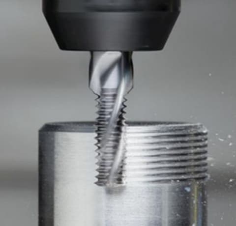
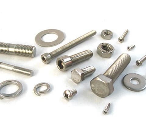
Hardware Installation Design Guidelines
Hardware installation adds threaded connection points, mounting features, and structural support directly to sheet metal parts. It is especially useful for thin sheet metal that is difficult to tap, a...
Mila
Sep 07,2026
1208
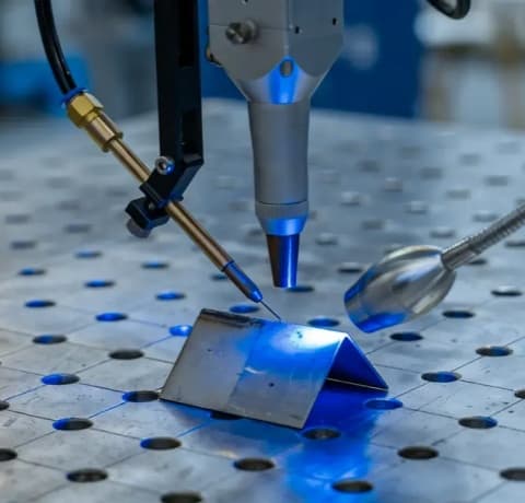
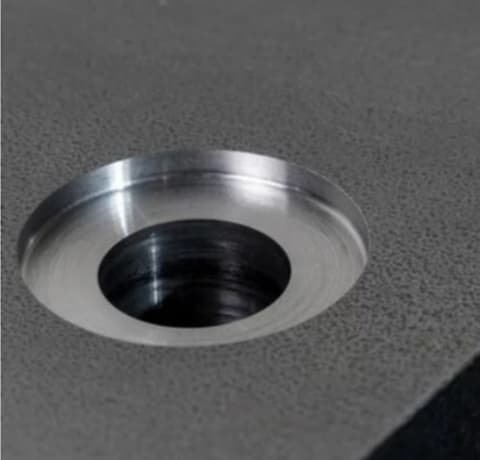
Countersink & Counterbore Holes Design Guidelines
This design guide provides structural engineers and mechanical designers with essential Design for Manufacturability (DFM) rules for Countersink (CSINK) and Counterbore (CBORE) holes in sheet metal fa...

Mila
Sep 03,2026
618
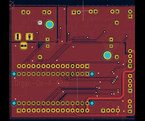
HDI PCB Layout Guide for High Speed Optical Module PCB Design
An optical module PCB is a typical high-frequency, high-density HDI PCB precision board. Its material selection is closely related to transmission rate, link length, loss budget, and device platforms....
Mila
Sep 02,2026
335
PCB Routing Angle Rules and the 90 Degree Trace Myth
In the realm of hardware design, "never use 90° angle traces" is one of the most widely circulated rules. Most engineers habitually modify 90° corners into 45° bends, or even intentionally increase tr...
Mila
Sep 01,2026
2104
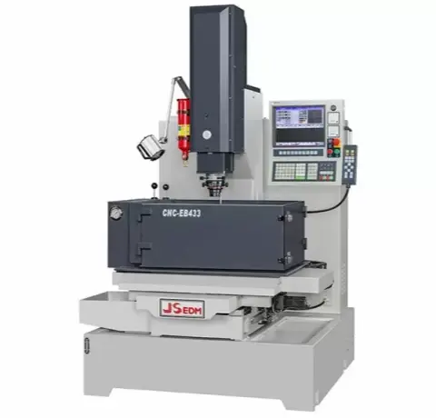
Electrical Discharge Machining (EDM) Design Guidelines
Electrical Discharge Machining (EDM) is a non-traditional machining process that uses controlled electrical discharges to remove material from electrically conductive workpieces. Because the electrode...

Mila
Aug 31,2026
778
PCB Impedance Control Guide: How to Fix Impedance Discontinuities in PCB Layout
In modern pcb design, maintaining signal integrity relies on a stable transmission path. Proper impedance control prevents signal reflection and ensures stable performance across your board. This arti...
Mila
Aug 28,2026
876
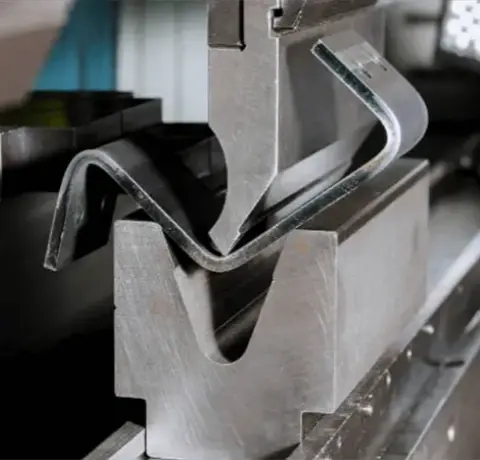
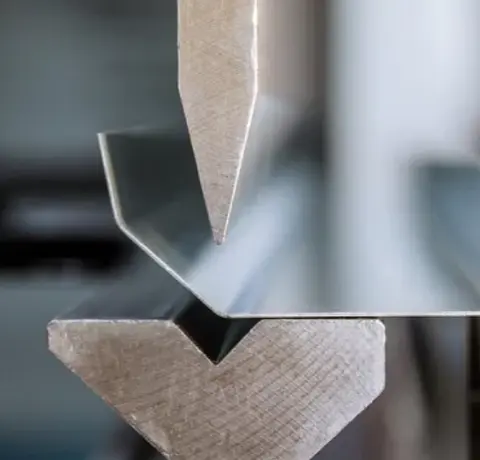
Sheet Metal Bending DFM Guide to Prevent Warping Tearing and Bending Deformation
In sheet metal bending and forming, warping, localized distortion, and corner tearing are common manufacturing defects. These issues typically stem from insufficient material support in the bend zone,...

Mila
Aug 28,2026
943
LDO Output Capacitor Selection: Why Bigger Isn't Always Better in Power Supply Design
In power supply design, there is a common engineering misconception regarding the selection of the LDO output capacitor: when faced with issues like high output ripple or poor load transient response,...

Mila
Aug 27,2026
786
PCB Routing Layer Selection for High-Speed Signals: Microstrip vs. Stripline
In the hardware layout for high-speed interfaces such as PCIe, DDR5, USB 3.0, and SerDes, selecting the trace layer—specifically choosing between surface microstrip and inner stripline—is a core decis...

Mila
Aug 26,2026
1053
Copper Keep-out Guidelines for PCB Layout and Component Layout
In modern pcb layout, solid copper pouring is widely used as an optimization technique. However, it is not universally applicable to all components. For devices whose magnetic fields easily couple wit...

Mila
Aug 25,2026
956
Power Supply Capacitor Layout: Placement Rules for Bulk and Small Capacitors
Engineers often encounter hard-to-spot issues when debugging switch-mode power supplies, DC-DC converters, and LDO circuits. These issues typically stem from placing electrolytic or tantalum bulk capa...

Mila
Aug 25,2026
1198
Ground Stitching Vias in High-Speed PCB Differential Via Design
In high speed PCB debugging, engineers frequently encounter high-speed link communications failure, severe eye diagram jitter, TDR impedance anomalies near via regions, and EMI radiation exceeding lim...

Mila
Aug 24,2026
490
High Speed PCB Design Guidelines for Impedance and SI
High-performance board layout is not merely about transmitting signals faster—it is about ensuring they remain stable, continuous, and predictable throughout the entire channel. As edge rates push int...

Mila
Aug 20,2026
1230
9 Essential PCB Copper Pour Techniques: A Complete Guide for PCB Layout Design
Copper pouring is a critical technique in PCB layout design that directly impacts signal integrity, thermal management, and manufacturing reliability. Whether you’re working on a high-speed digital bo...

Mila
Aug 18,2026
871
Industrial-Grade RS-485 Communication Interface Design and PCB Layout
1. Introduction: An Irreplaceable Foundation of Industrial Bus CommunicationIn industrial automation, medical equipment, and smart grid applications, the stability of communication interfaces directly...
| Ranking | Name | Answers |
|---|---|---|
| 1 | PCBWay Team | 12 |
| 2 | Engineer | 1 |
| 3 | SAAD ZAFAR | 1 |