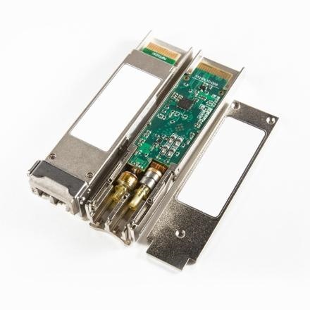
An optical module PCB is a typical high-frequency, high-density HDI PCB precision board. Its material selection is closely related to transmission rate, link length, loss budget, and device platforms. While 10G and lower modules can use materials like high-Tg FR-4, high-speed modules operating at 25G, 56G, 100G, 400G, and 800G impose stringent requirements on low-loss materials, impedance control, and manufacturing consistency.
Below are seven core layout design points and key differences compared to standard PCBs, focusing on high speed pcb layout and practical signal integrity engineering without rigid design fallacies.
1. Substrate Selection and StackUp Design
Substrate selection and layer stackup form the foundation for stable high-frequency transmission, directly determining link insertion loss, impedance accuracy, and signal integrity.
- Multi-Dimensional Rate-Matched Selection: For 25G+ channels, select substrates considering Nyquist frequency, link length, insertion loss budget, dielectric loss, copper foil roughness, and stackup. For long-distance or low-loss channels, choose mid-to-low loss high-speed substrates. Non-critical areas like low-speed control and power can use high-Tg FR-4 to balance performance and cost on an optical module PCB.
- Adjacent Reference Ground Planes: High-speed differential signal layers should adopt a "signal-reference ground" structure to minimize edge-field coupling. Power layers should pair with adjacent ground layers to optimize PDN impedance via inter-layer capacitance.
- Pre-Simulation Impedance Modeling: Determine stackup parameters early through SI simulation. The industry standard target is typically 100 ohms differential impedance, with high-performance channels strictly controlling tolerances within +/- 5%.
2. High-Speed Differential TX/RX Signal Integrity
High-speed differential signals are the core of data transmission in an optical module PCB. Design should focus on eliminating geometric discontinuities and parasitic interference.
- Symmetry and Equal Length: Match trace widths, spacing, bends, and via layouts for differential pairs. Advanced HDI pcb design requires controlling intra-pair length skew to prevent differential-to-common mode noise conversion.
- Trace Geometry Continuity: Use 45-degree angles or smooth arc transitions instead of rigid 90-degree turns. High-frequency reflections stem mostly from vias, pads, stubs, and split reference planes rather than standard trace corners.
- Minimal Via Structures and Stub Optimization: Minimize layer transitions. For long through-hole structures, apply back-drilling to remove residual stubs, cutting down reflections and resonances.
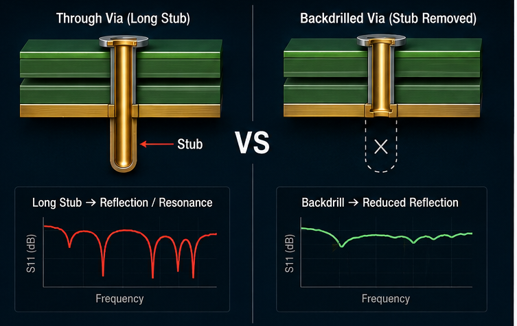
(Backdrill + Via Stub)
- Unbroken High-Frequency Return Paths: Avoid routing differential traces across ground splits or slot gaps. Provide nearby stitching ground vias whenever signals switch layers.
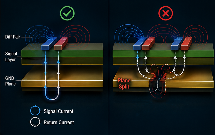
(Differential Pair + Reference Plane + Return Path)
- Crosstalk Mitigation: Apply the 3W rule during initial layout for proper spacing. For 112G PAM4 ultra-high-speed scenarios, refine trace spacing with 3D EM simulation and add ground via shielding walls where necessary.
3. Optoelectronic Isolation and Sensitive Layout
Optical modules combine sensitive analog signals with high-speed digital logic. The analog front-end requires isolation from power and digital noise.
- Physical Isolation: Separate TOSA/ROSA components and TIA analog circuits from high-speed digital traces and switching power supplies based on form factors (SFP, QSFP, OSFP).
- Short Analog Traces: Keep weak analog traces from optical devices to TIA and driver ICs as short as possible, avoiding parallel routing alongside high-speed digital lines.
- Analog Circuit Shielding: Implement localized ground shielding or small metal shields around laser drivers and TIA circuits to isolate high-frequency digital noise.
4. Power Integrity (PI) Optimization
Focus on low-impedance return paths, minimal current loops, and sub-region noise reduction.
- Minimal Loop Decoupling: Configure decoupling networks based on target PDN impedance. Place capacitors close to power pins to minimize parasitic inductance.
- Solid Ground Plane Priority: Maintain a continuous, low-impedance ground plane across the HDI PCB to provide a solid reference. Apply localized filtering for sensitive analog zones rather than single-point star grounding across the board.
- Thermal Copper Pour for Power Chips: Place large copper areas with thermal via arrays beneath heat-generating components like laser drivers to disperse heat quickly.
Optical module DSPs, optical drivers, and laser diodes generate concentrated heat. High temperatures cause device aging, DK/Df parameter drift, and impedance shifts.
- Efficient Thermal Paths: Place dense thermal via arrays under high-power devices (DSP, TOSA) to transfer heat from the optical module PCB inner layers to the metal housing.
- Hot/Cold Component Partitioning: Isolate heat sources from temperature-sensitive optical and clock components to prevent thermal drift and premature aging.
- Symmetrical Design against Warpage: Balance copper distribution and layer stack-ups across the HDI PCB to manage thermal-mechanical stress during reflow soldering.
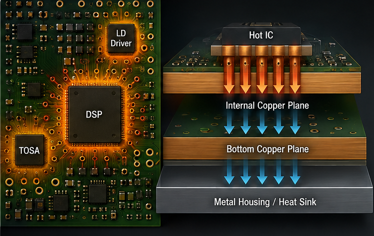
(Thermal Path IC → Thermal Via → Copper Plane → Housing)
- Symmetrical Routing for Common-Mode Noise: Maintain structural symmetry in high-speed differential traces to reduce EMI radiation. Connect the module metal shell to the PCB ground for low-impedance shielding.
- Interface ESD Protection: Place TVS diodes and common-mode chokes near edge connectors to route ESD currents quickly to chassis ground.
- Isolate Interference Sources: Keep power inductors and switching regulators away from sensitive RX analog inputs to prevent magnetic coupling.
7. DFM Guidelines for Optical Module PCB Manufacturing
Precise HDI pcb design and assembly standards ensure manufacturing yield for dense components.
- Precision Soldering Design: Use Via-in-Pad or micro-vias for high-density BGAs. For QFN thermal pads, use segmented stencil openings to reduce solder voiding and floating.
- Optical Alignment Tolerance: Match mechanical outline and mounting hole tolerances precisely with metal housings to avoid optical misalignments.
- Test Points and Gold Fingers: Keep test points off high-speed trunk lines. Use hard gold plating for edge connector gold fingers to ensure durability across insertion cycles.
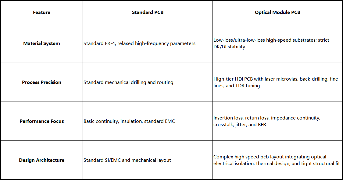
8.Optical Module PCB vs Standard PCB Core Differences