 Mila
Sep 16,2025
8234
PCB Layout Design Process from Schematic to Manufacturing
PCB layout design is the process of transforming an electrical schematic into a complete, manufacturable printed circuit board (PCB). A well-designed PCB layout must do more than simply connect compon...
Mila
Nov 09,2026
52
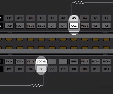
USB Type-C Pinout: Why Are 5.1KΩ Pull-Down Resistors Needed?
USB Type-C has become a common interface in modern electronic devices thanks to its reversible design, high-speed data transfer, and high-power delivery capabilities. However, in USB Type-C circuit de...
PCBWay
Nov 09,2026
160
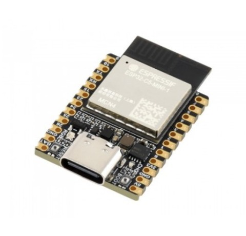
PCBWay Store NewArrival Product - ESP32-C5 Mini Dual-band Development Board
Link:ESP32-C5 Mini Dual-band Development BoardESP32-C5 dual-band Wi-Fi 6Development BoardSupports ESP-IDF, Arduino IDE, etc.Onboard ESP32-C5-MINI-1 Series Module version optionsESP32-C5-MINI-KITO...
Mila
Nov 06,2026
101
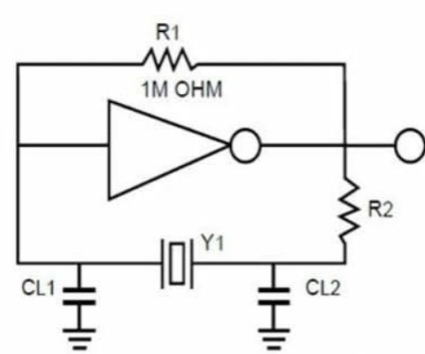
Clock Circuit Design Guidelines for PCB Layout
Clock circuits play an essential role in electronic systems by providing timing signals that synchronize the operation of different components. However, improper clock circuit design can lead to signa...
Mila
Nov 04,2026
303
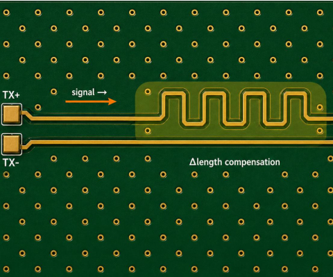
Differential Pair Routing: 3 Common Design Mistakes to Avoid
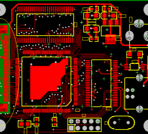
In high-speed PCB design, differential pairs are increasingly used, especially in high-speed interfaces such as USB, HDMI, and PCIe. These interfaces commonly use differential signaling for reliable d...
Mila
Nov 04,2026
329
PCB Layout Guidelines for Better Soldering Quality
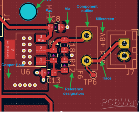
PCB design plays an important role in soldering quality and overall assembly reliability. From component placement and pad design to fiducial marks and copper connections, even small layout details ca...
Mila
Oct 29,2026
525
12 PCB Layout Guidelines for Better Component Placement
PCB layout involves more than simply placing components and routing traces. Component spacing, decoupling capacitor placement, pad connections, thermal management, and manufacturing constraints all af...
Mila
Oct 28,2026
483
Notice for AI-Generated Design Files and Manufacturing Requirements
Now AI tools can help customers generate PCB, PCBA, 3D printing, and CNC machining designs, along with detailed manufacturing notes and documentation. However, AI-generated submissions may contain exc...
Mila
Oct 27,2026
597
PCB Layout Considerations for Single-Point and Multi-Point Grounding
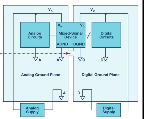
PCB grounding is an important part of PCB layout, affecting circuit stability, noise levels, signal integrity, and electromagnetic compatibility (EMC). Different circuits have different grounding requ...
PCBWay
Oct 27,2026
886
PCBWay Store NewArrival Product - Industrial 1-Channel ESP32-S3 WiFi Relay Module
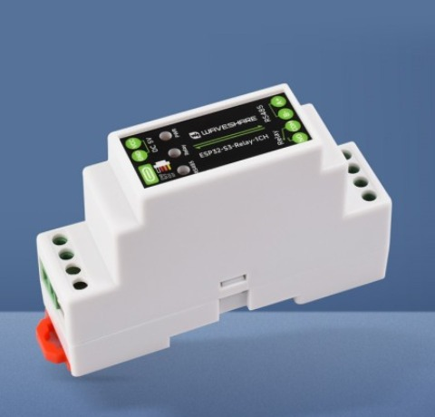
Link:1-CH ESP32-S3 WiFi Relay ModuleBased on ESP32-S3, Supports Wi-Fi / Bluetooth, Onboard RS485 interfaceBuilt-in protection circuits such as power isolation and optocoupler isolation, Safe & Sta...
Mila
Oct 26,2026
387
PCB Layout Guidelines for Special Component Placement
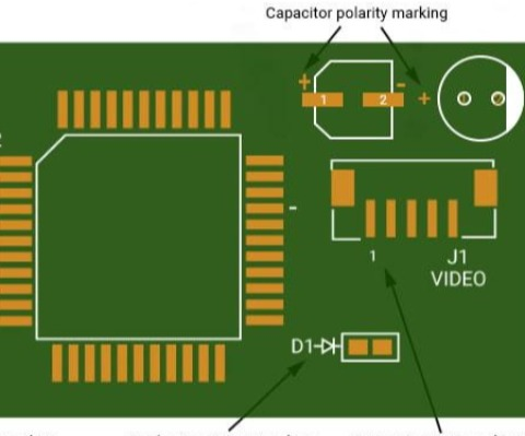
PCB layout is not an arbitrary process. It must follow certain design rules to ensure electrical performance, thermal management, and assembly quality. In addition to general layout requirements, some...
Mila
Oct 26,2026
680
PCB Copper Thickness Guide for Current, Impedance, and Heat Dissipation
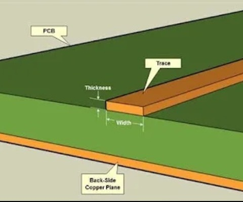
PCB copper thickness affects current-carrying capacity, trace impedance, heat dissipation, and manufacturing complexity. Thicker copper is not always better, and thinner copper is not always the right...

Mila
Oct 22,2026
445
PCB Routing Guidelines for Ground, Power, and Signal Traces
Poor PCB routing can lead to signal integrity issues, EMC failures, and power instability, even when component selection and schematic design are correct. These problems often stem from discontinuous ...

Mila
Oct 21,2026
1776
How to Get $29 PCB Assembly and Meet the Requirements
PCBWay's $29 PCB assembly offer provides a special assembly service price for eligible PCB prototypes. It is designed for relatively simple projects with limited assembly requirements.Not every PCB as...
Mila
Oct 20,2026
313
How to Design a Ground Guard Trace in PCB Design
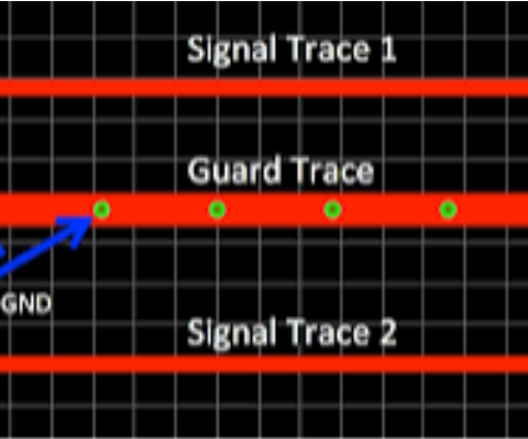
In PCB design, a ground guard trace is a copper trace connected to ground and placed alongside a signal trace or around a sensitive circuit area. It can help reduce unwanted capacitive coupling and el...
Mila
Oct 19,2026
1080
Power Supply Pinout Explained: VIN, VOUT, SW, PH, and BAT
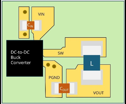
Isn’t VIN the power input and VOUT the output? Many beginner hardware engineers have this question in PCB layout when they first look at power ICs and power module schematics. If a power supply essent...
| Ranking | Name | Answers |
|---|---|---|
| 1 | PCBWay Team | 2 |