PCB layout is not an arbitrary process. It must follow certain design rules to ensure electrical performance, thermal management, and assembly quality. In addition to general layout requirements, some components have specific placement constraints that must be considered during PCB component placement.
For right-angle male and female press-fit components, no components taller than 3 mm should be placed within 3 mm of the component, and no soldered components should be placed within 1.5 mm. On the opposite side of the PCB, no components should be placed within 2.5 mm of the center of the press-fit pin holes.
For straight male and female press-fit components, no components should be placed within 1 mm of the component. If a protective sleeve is required on the opposite side of the PCB, no components should be placed within 1 mm of the sleeve edge. If no sleeve is installed, no components should be placed within 2.5 mm of the press-fit holes.
For hot-plug sockets used with grounding connectors in European-style connectors, components should not be placed within 6.5 mm of the front end of long pins or within 2.0 mm of the front end of short pins.
For long pins on 2 mm FB single-pin power connectors, no components should be placed within 8 mm in front of the corresponding board-mounted socket.
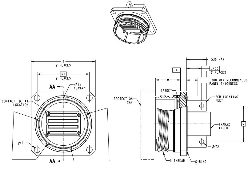
(Press-Fit Connector Placement and Clearance Requirements)
During PCB component placement, temperature-sensitive components should be kept away from high-heat components whenever possible. For example, electrolytic capacitors should be protected from prolonged exposure to excessive temperatures, while crystal oscillators require attention to temperature variations that may affect frequency stability.
Components used for temperature sensing should be placed according to the target being measured and the actual heat-transfer path. They should be positioned to accurately reflect the target temperature while minimizing the influence of other heat-generating components, which could otherwise cause measurement errors or false triggering.
Heat-generating components that can withstand high temperatures should be placed in locations that support effective heat dissipation, taking the actual airflow path into account. Components with limited heat resistance should be kept away from high-temperature areas. Where possible, avoid placing them directly in the airflow path downstream of other heat-generating components or where they may affect temperature-sensitive components.
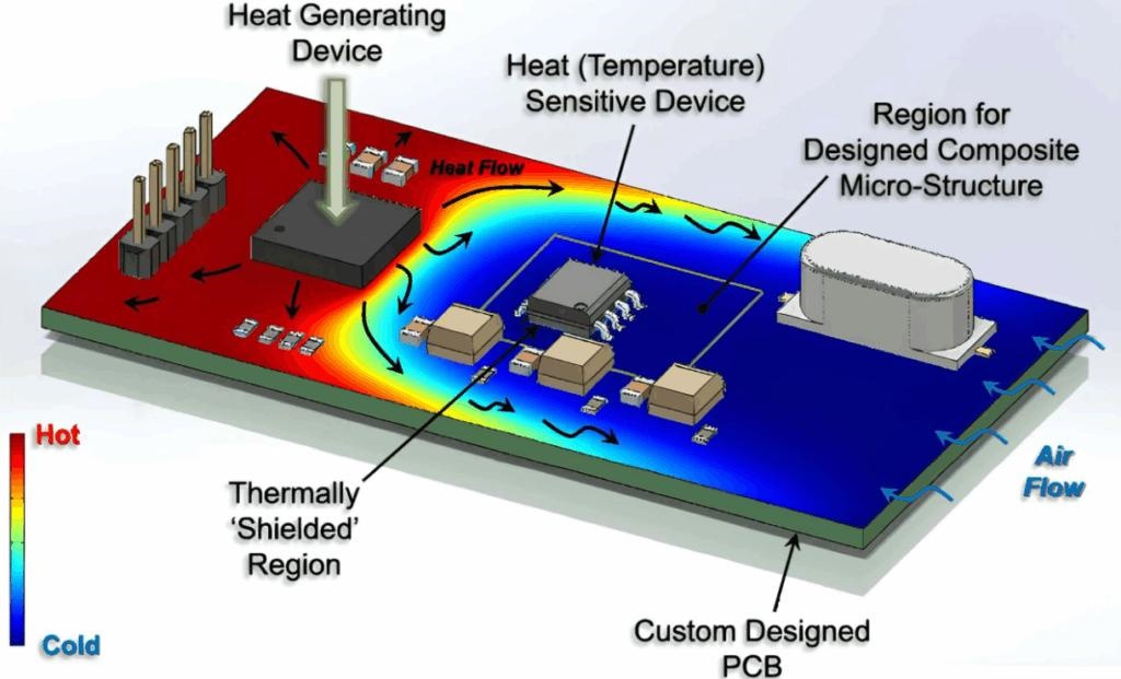
(PCB Layout for Thermal-Sensitive Components)
Common polarized components include electrolytic capacitors, tantalum capacitors, and diodes. During PCB layout, always verify component polarity markings against the schematic and PCB footprint to prevent circuit malfunctions caused by incorrect orientation.
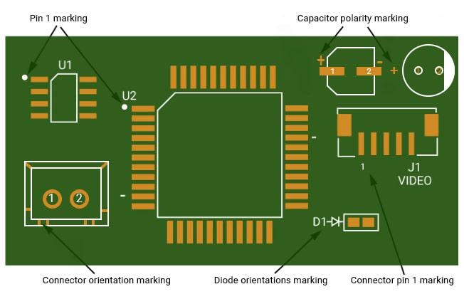
(Polarized Component Orientation in PCB Layout)
Proper PCB layout affects not only electrical performance but also thermal management, assembly efficiency, and product reliability. When developing PCB component placement guidelines, designers should consider component characteristics, electrical requirements, mechanical clearances, and manufacturing processes. Reviewing these factors against component datasheets and assembly requirements can help prevent placement conflicts, reduce manufacturing issues, and improve overall PCB design quality.