PCB design plays an important role in soldering quality and overall assembly reliability. From component placement and pad design to fiducial marks and copper connections, even small layout details can affect solder paste printing, component placement, and reflow soldering. In this article, we'll explore key PCB layout guidelines to help reduce common soldering defects and improve SMT assembly efficiency.
Producing a high-quality PCB assembly involves multiple stages, from PCB design to component soldering. It requires coordination among PCB designers, process engineers, and production personnel.
Several factors can affect PCB soldering quality, including PCB design files, board quality, component quality, oxidation on component leads, solder paste quality, solder paste printing accuracy, pick-and-place programming and placement accuracy, and the reflow oven temperature profile.
Among these factors, PCB layout is one of the important elements that directly influence downstream assembly processes.
PCB designers may have limited hands-on soldering and manufacturing experience, while production operators at assembly facilities are generally more focused on manufacturing tasks than on analyzing PCB design decisions. If manufacturing and soldering requirements are not considered during the design stage, unnecessary production difficulties may arise.
Therefore, PCB designers should consider assembly processes and manufacturing requirements from the beginning to minimize potential problems during production.
The following guidelines cover practical PCB layout considerations that can help reduce soldering defects and improve SMT assembly and repair efficiency.
For PCBs that require SMT assembly, tooling holes can be added according to the requirements of the production equipment. They help secure and position the board during solder paste printing and subsequent manufacturing processes.
Tooling holes are generally placed near the board corners or on the tooling edges. When multiple holes are used, their relative positions and machining accuracy should be carefully controlled to avoid positioning errors during production.
The number, diameter, and location of tooling holes should be determined based on the PCB dimensions, panelization method, and equipment requirements. Four tooling holes at the corners are not mandatory for every PCB.
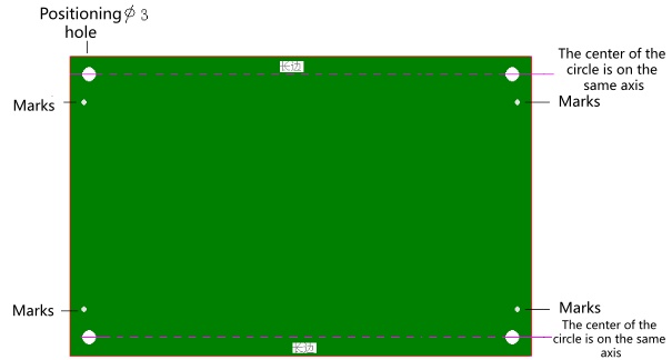
Fiducial marks should be provided on the PCB when required by the SMT equipment. They allow the pick-and-place machine to recognize the board's position and orientation through its vision system, improving component placement accuracy.
Fiducial marks are commonly placed diagonally across the PCB and typically use circular exposed copper patterns. Sufficient clearance should be maintained around each mark to prevent nearby copper, pads, or silkscreen graphics from interfering with visual recognition.
For double-sided SMT assembly, fiducial marks may be required on both sides, depending on the equipment and assembly process.
For panelized PCBs, additional fiducial marks can also be placed on the tooling edges or panel to help the machine identify the entire panel.
When designing fiducial marks, consider the following points:
a. Fiducial marks generally use solid circular exposed copper patterns. Their shape and dimensions should meet the requirements of the pick-and-place machine.

b. A typical fiducial mark diameter is approximately 1.0 mm, although the exact size should follow the equipment manufacturer's specifications.
c. Maintain a sufficient clearance around each fiducial mark. Avoid placing copper features, pads, silkscreen, or other patterns within this area. A clearance of approximately 1.0 mm around the mark is commonly used, subject to equipment requirements.
d. The fiducial mark should provide sufficient contrast against the surrounding PCB surface to ensure reliable visual recognition.
e. Keep the fiducial surface clean and flat. Oxidation, contamination, or excessive reflection may affect recognition accuracy. Exposed copper is commonly used, with the surface finish selected according to the PCB manufacturing process.
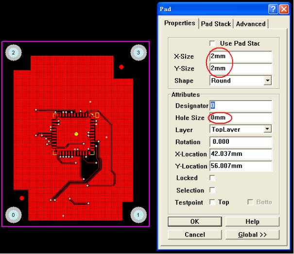
Note that simple silkscreen outlines should not be used as substitutes for fiducial marks. Pick-and-place machines need to recognize a physical feature with a clearly defined boundary and optical characteristics.
PCB layouts should account for the conveying and clamping requirements of SMT equipment.
For boards transported along conveyor rails, sufficient component-free space should be maintained near the board edges to prevent components from interfering with the rails or fixtures. Depending on the equipment, a clearance of approximately 3–5 mm from the board edge may be used as a reference.
Avoid placing SMD components, protruding pads, or other features that may interfere with board handling in this area.
For double-sided SMT assembly, also consider the risk of component movement or falling during the second reflow process, as well as potential interference between components and conveyor rails.
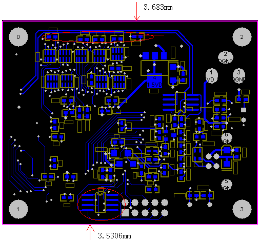
If the PCB is too small to provide sufficient edge clearance, consider adding tooling edges to provide space for board transportation, positioning, and clamping.
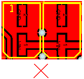
If an untreated via is placed directly within a conventional SMD pad, molten solder may flow into the via during reflow soldering. This can result in insufficient solder at the joint and, in severe cases, lead to weak or unreliable connections.
Therefore, vias should generally be avoided directly within ordinary SMD pads.
However, Via-in-Pad structures may be necessary for high-density layouts or specific component packages. In such cases, processes such as resin filling and copper capping can be used to prevent solder loss.
Polarized components, such as diodes and tantalum capacitors, should have clearly defined polarity markings on the PCB to prevent incorrect placement during assembly or manual soldering.
Polarity indicators must match the pin definitions in the component datasheet. Standard industry symbols should be used whenever possible.
Even when PCB space is limited, ensure that polarity markings remain visible and are not covered by component bodies or other silkscreen graphics.
PCB silkscreen should be clear and concise. Avoid excessive component models, specifications, and other text that may make the board difficult to read, especially in high-density layouts.
Component reference designators, such as R1, C1, and U1, should be retained whenever possible. They help production personnel identify component locations and make inspection and repair easier.
Do not use component descriptions or part numbers without reference designators. This may increase the difficulty of pick-and-place programming and component identification during production.
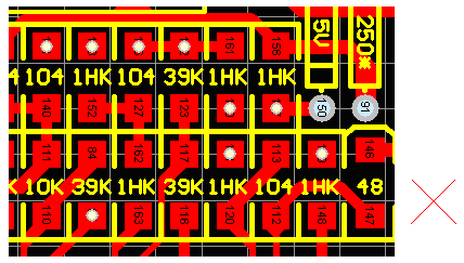
In addition, silkscreen text should not be too small. Place characters away from vias, pads, and other features that may interfere with readability.
For IC packages with exposed leads, such as SOP, PLCC, and QFP, pad length should be determined based on the component lead dimensions and recommended footprint design.
Appropriate pad dimensions help ensure proper solder paste printing, solder wetting, and reliable joint formation. They can also provide sufficient access for manual soldering and rework.
However, using a fixed ratio, such as 1.5 times the IC lead length, is not recommended as a universal rule. Different package types have different lead structures and dimensions.
Always refer to the recommended land pattern in the component datasheet or relevant IPC footprint design guidelines.
For IC packages such as SOP, PLCC, and QFP, pad width and the spacing between adjacent pads directly affect soldering quality.
Follow the recommended footprint dimensions in the component datasheet when determining pad width and spacing.
Pads that are too wide or have insufficient spacing between them may increase the risk of solder bridging during assembly.
For fine-pitch IC packages in particular, careful attention should be paid to pad dimensions, solder paste printing accuracy, and solder mask design.
During PCB layout, pay attention to component orientation and rotation angles. Keeping components of the same type oriented consistently can simplify pick-and-place programming, inspection, and maintenance.
It is worth noting that modern pick-and-place machines generally support arbitrary component rotation angles and are not limited to 90°, 180°, or 270° increments.
However, component rotation must be consistent with the footprint definition, coordinate files, and placement program. Otherwise, component leads may become misaligned with PCB pads, affecting placement and soldering quality.
Pay particular attention to polarity when positioning diodes, electrolytic capacitors, and other polarized components.
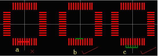
When adjacent IC pins need to be electrically connected, the PCB layout should be designed carefully to avoid soldering problems and make inspection easier.
Avoid simply merging multiple pad areas into one large copper region.
Instead, use appropriate routing connections and solder mask openings according to the electrical requirements. Ensure that the soldering areas of individual pins remain clearly defined.
Sufficient clearance must be maintained between pads that should not be electrically connected to prevent solder bridging.
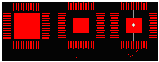
Some IC packages, such as QFN and DFN, have an exposed thermal pad on the underside of the component. This pad is mainly used for heat dissipation and electrical grounding.
When designing these packages, follow the recommended thermal pad dimensions in the component datasheet and consider the solder paste stencil design.
If the thermal pad is too large and the entire area is covered with solder paste, excessive solder paste may cause problems such as solder voiding, component floating, or solder overflow during reflow.
To reduce these risks, the solder paste opening can be divided into multiple smaller sections to control the amount of solder paste deposited.
However, the thermal pad should not be arbitrarily reduced simply to prevent short circuits. Thermal performance, electrical connections, and soldering requirements must all be considered.
Component height and spacing should be considered during PCB layout. If two tall components are placed too close together, the pick-and-place machine may encounter interference when positioning the second component. The first component may obstruct the placement head or nozzle, affecting the placement process.
Overcrowded layouts can also make inspection, soldering, and rework more difficult.
Therefore, consider component height, package dimensions, nozzle clearance, and maintenance requirements when arranging taller components. Provide sufficient spacing to avoid mechanical interference.
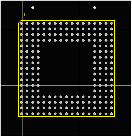
BGA components have solder balls underneath the package. Since these solder joints cannot be directly inspected from the outside after assembly, BGA packages require careful attention to PCB pad design, solder paste printing, and reflow soldering.
When designing BGA footprints, strictly follow the component datasheet recommendations for pad dimensions, ball pitch, and PCB layout requirements.
It is also important to consider inspection and rework requirements in advance. For example, additional positioning features may be needed on the PCB to accommodate BGA rework equipment and fixtures.
If auxiliary tooling holes are required, their diameter, location, and spacing should match the actual rework equipment or alignment fixture. A single hole size should not be applied to every BGA design.
Although solder mask color does not directly determine soldering quality, it may affect the visual recognition performance of SMT equipment.
Different solder mask colors have different optical and reflective characteristics, which may influence how the machine's vision system recognizes fiducial marks and component positions.
For example, certain dark solder mask colors may provide insufficient contrast under specific lighting conditions.
Therefore, when selecting a PCB color, consider not only appearance but also compatibility with the production equipment's vision system. For unusual solder mask colors, confirm compatibility with the PCB manufacturer and SMT assembly provider in advance.
During PCB layout, avoid placing small components underneath large components when doing so may obstruct soldering, inspection, or rework.
For example, if resistors or capacitors are placed underneath a seven-segment display or a large connector, technicians may need to remove the larger component before repairing the smaller one if a soldering defect occurs.
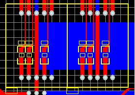
This increases repair complexity and may damage the larger component or nearby pads during removal.
Therefore, when circuit functionality and routing requirements allow, consider placing some small components on the opposite side of the PCB or repositioning them to provide better access for inspection and repair.
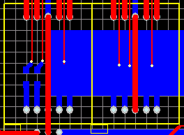
When a PCB pad is directly connected to a large copper pour, heat may dissipate more rapidly during soldering. This can slow down pad heating and affect solder melting and wetting.
This is particularly relevant for pads connected to large copper planes or internal power and ground layers.
For example, in Figure A, the component pad is directly connected to a large copper area. In Figure B, although the connector pad is not directly connected to the copper pour, the large copper planes in the inner layers may still increase the overall thermal mass and affect soldering.
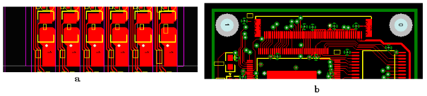
If the reflow temperature is increased to compensate for excessive heat dissipation, temperature-sensitive connectors or plastic components may become deformed.
Therefore, for pads that do not require direct high-current connections or special thermal performance, consider using thermal relief connections. These connections use narrow copper spokes to reduce heat dissipation and improve solderability.
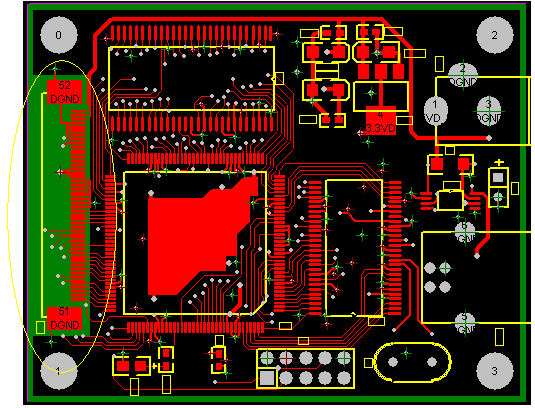
For high-current pads and thermal pads, however, current-carrying capacity, heat dissipation, and soldering requirements must be considered together. Thermal relief should not be applied indiscriminately.

For small or irregularly shaped PCBs, panelization can improve SMT production efficiency by allowing multiple boards to be processed together.
Several factors should be considered when designing PCB panels:
A well-designed PCB panel can improve SMT production efficiency while reducing positioning errors and mechanical damage during assembly.
PCB layout should consider not only circuit functionality and electrical performance but also downstream manufacturing, soldering, inspection, and repair requirements.
Proper fiducial mark placement, pad design, component arrangement, and panelization can help reduce potential problems during solder paste printing, SMT placement, and reflow soldering.
PCB designers should therefore take actual manufacturing processes into account from the early design stage. A well-designed PCB should not only meet electrical requirements but also be easy to manufacture and assemble.