In high-speed PCB design, differential pairs are increasingly used, especially in high-speed interfaces such as USB, HDMI, and PCIe. These interfaces commonly use differential signaling for reliable data transmission.
Why is differential signaling so widely used? Compared with conventional single-ended routing, differential pairs offer better noise immunity, help suppress common-mode noise and electromagnetic interference (EMI), and improve signal integrity and timing performance.
In PCB design, a differential pair consists of two closely coupled signal traces. To ensure signal transmission quality, these traces generally need to have matched lengths, equal widths, consistent spacing, and symmetrical routing. Differential impedance must also be controlled according to the design requirements.
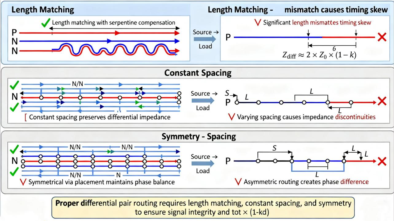
(Differential Pair Routing Requirements)
Equal length means keeping the two traces in a differential pair as close in length as possible. The purpose is to control the propagation delay difference (skew) between the two signals, maintain proper timing alignment, and reduce signal imbalance and the resulting common-mode noise.
Equal width means maintaining the same trace width for both signals. Equal spacing means keeping the distance between the two traces as consistent as possible, allowing them to run symmetrically and in parallel.
This helps maintain a stable coupling relationship between the two traces, minimizes differential impedance variations, and improves signal transmission quality.
When designing a PCB with differential pairs, one of the first steps is to determine the target differential impedance required by the interface and plan the routing accordingly.
It is also important to minimize impedance variations along the routing path. Differential impedance is affected by several factors, including trace width, spacing between the two traces, copper thickness, PCB material, and stackup structure. These factors should all be considered during the design process to maintain consistent differential impedance.
Although differential signals offer strong noise immunity, they still require an appropriate reference plane. The reference plane beneath the differential pair should remain continuous whenever possible. Avoid routing differential pairs across split ground planes or slots in the reference plane, as these discontinuities can alter return paths and cause impedance variations.
Differential signals offer strong immunity to common-mode noise, but this does not mean they do not need a reference plane.
In fact, the return-current path depends on the coupling between the two differential traces and their coupling to the reference plane. Differential-mode return current is primarily associated with the electromagnetic coupling between the two traces, while the reference plane still affects the return path and impedance characteristics, especially for common-mode currents.
When the reference plane contains splits or slots, the return-current path may change, causing impedance discontinuities, signal degradation, and increased EMI. Therefore, differential pairs should be routed over a continuous reference plane whenever possible, avoiding split ground regions.
In addition, removing the reference plane beneath differential traces to suppress common-mode noise is not recommended. This can make impedance control more difficult and disrupt the return path for common-mode currents, potentially increasing electromagnetic radiation.
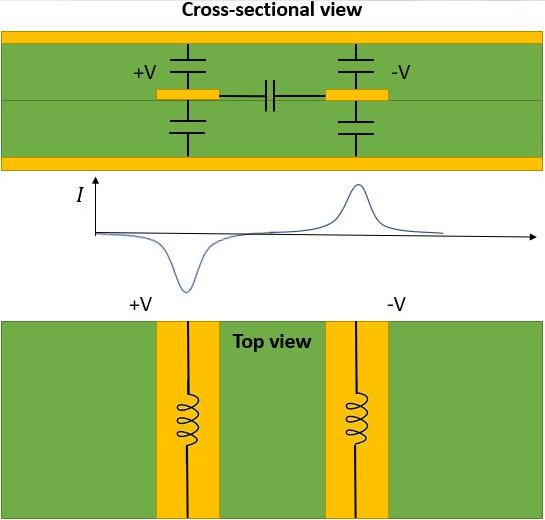
(Differential Signal Reference Plane)
In practical PCB routing, it is not always possible to satisfy every differential pair design requirement simultaneously. Component pin placement, via locations, and available routing space may require designers to introduce serpentine routing to match trace lengths. However, this can cause some sections of the differential pair to lose their parallel alignment or consistent spacing.
In such cases, design priorities should be determined according to the interface specifications and application requirements. For high-speed differential interfaces with strict intra-pair skew limits, length matching is particularly important. However, trace spacing also affects coupling and differential impedance, so it should not be overlooked.
During routing, priority should be given to meeting interface timing and impedance requirements. Symmetry, consistent spacing, and routing continuity should then be maintained as much as possible, rather than focusing on just one routing parameter.
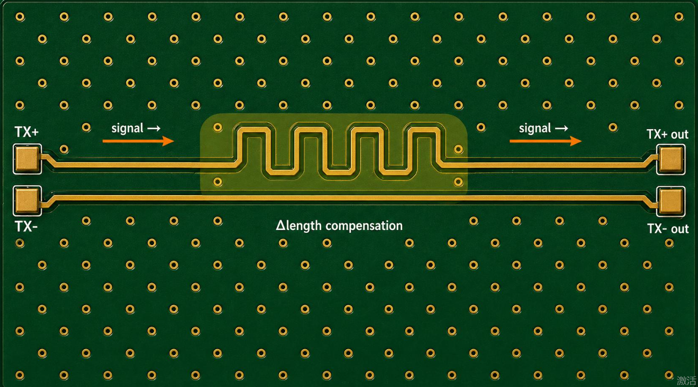
(Differential Line Length Matching)
Routing differential traces close together strengthens the coupling between them, improving noise immunity and helping reduce electromagnetic radiation through partial magnetic field cancellation.
However, closer spacing is not always better. The spacing should be determined by the target differential impedance, PCB stackup, and application requirements. Excessively small spacing may make impedance control and manufacturing more challenging.
To reduce crosstalk, maintain sufficient spacing between differential pairs and other signal traces. The 4W rule (spacing of at least four times the trace width) can serve as an initial guideline, but actual spacing should be determined by the design requirements.
Ground guard traces connected to the reference plane through stitching vias can also provide additional isolation. For high-frequency applications, coplanar waveguide (CPW) structures are another option for controlling differential impedance.
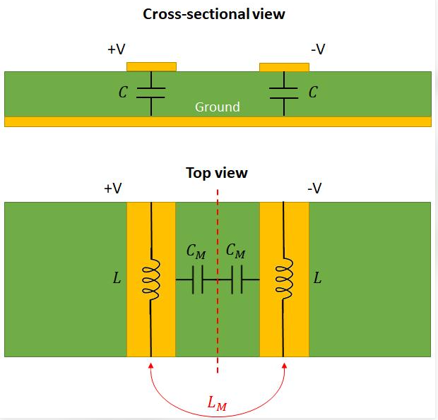
(Differential Line Spacing)
Differential pair routing is an important part of high-speed PCB design. In addition to trace length, width, and spacing, designers must also consider differential impedance, reference-plane continuity, and interference from surrounding signals. Only by considering all these factors together can designers ensure reliable differential signal transmission and improve overall PCB performance and reliability.