Clock circuits play an essential role in electronic systems by providing timing signals that synchronize the operation of different components. However, improper clock circuit design can lead to signal interference, timing errors, and system instability. This article explores the PCB design guidelines for crystal circuits, active oscillators, and clock distributors, covering key considerations for component placement, signal routing, and noise reduction.
A clock is an essential part of any electronic system. It acts like the heartbeat of the system, providing synchronization signals to different components. If the clock signal becomes unstable or fails, the entire system may malfunction or stop working. Therefore, proper clock circuit design is essential in PCB design.
Common clock sources and distribution components used in PCBs include crystals, oscillators, and clock distributors. Some ICs may generate their own clock signals internally. However, the clock signal ultimately originates from a crystal, an oscillator, or another clock source before being distributed to other components.
When designing a crystal circuit, consider the following guidelines:
Common crystal packages used in PCB design include 2-pin through-hole packages, 2-pin SMD packages, and 4-pin SMD packages.
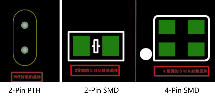
(Common crystal package types)
Although crystals are available in different package sizes and specifications, their basic operating principles and peripheral circuit designs are similar. Therefore, many PCB placement and routing guidelines are applicable across different crystal designs. A basic crystal circuit is shown below:
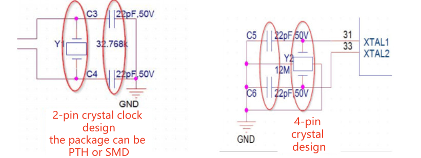
(Basic crystal circuit schematic)
The two capacitors shown in the schematic are load capacitors. They connect the two crystal terminals to ground and provide the required load capacitance for stable oscillation. Their values should be determined based on the crystal datasheet, the IC's internal oscillator characteristics, and the parasitic capacitance of the PCB.
When placing a crystal circuit, position the two load capacitors as close as possible to the crystal and the IC's oscillator pins. This helps minimize trace length and reduce the impact of parasitic parameters.
The placement is shown below:
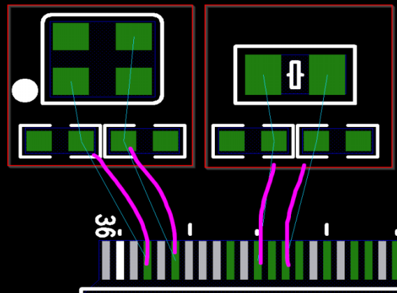
(Crystal circuit placement)
When routing the crystal circuit, keep the two connections between the crystal and the IC as short as possible and preferably close to each other to reduce parasitic capacitance and external interference.
Note that these two traces are not true differential signal lines, so differential routing rules should not be applied directly.
Avoid unnecessary vias and follow the IC manufacturer's layout recommendations to determine whether GND guard traces are needed.
The routing layout is shown below:
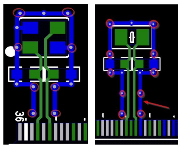
(Crystal circuit routing)
The circuit described above is the most basic and commonly used crystal circuit design. In practical PCB designs, additional components such as series resistors and test points may be included to meet debugging or signal integrity requirements. However, the basic design principles remain the same.
Based on the guidelines above, consider the following points when placing components:
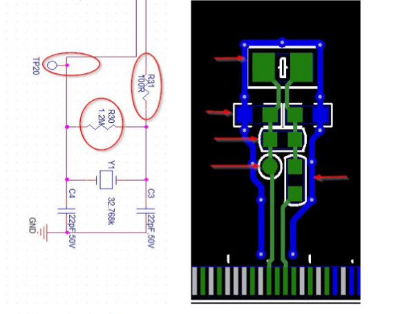
(Crystal circuit layout with a series resistor and test point)
Routing guidelines:
Unlike passive crystals, active oscillators integrate an internal oscillation circuit and can directly output clock signals.
An active oscillator circuit typically consists of an oscillator device, a power supply decoupling circuit, and an optional source-series resistor selected according to the output interface and load requirements.
A typical oscillator circuit is shown below:
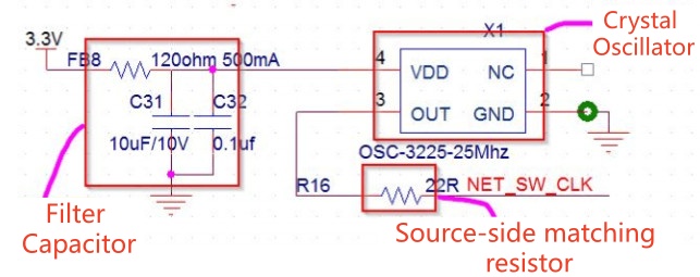
(Active oscillator circuit schematic)
The PCB placement and routing layout is shown below:
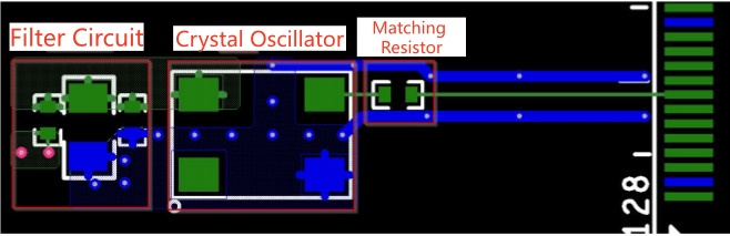
(Active oscillator PCB layout and routing)
Placement and routing guidelines:
A clock distributor is primarily used to distribute a clock signal from a clock source to multiple ICs or functional modules. Different clock distributors vary in terms of output count, frequency range, output interface, and drive capability.
During PCB design, carefully plan the placement of the clock distributor relative to the receiving ICs to minimize clock signal routing distances. For designs that require clock skew control, also consider the routing lengths and loads of different output channels. The clock distributor is often placed at a relatively central position among the receiving devices.
A typical clock distributor circuit is shown below:
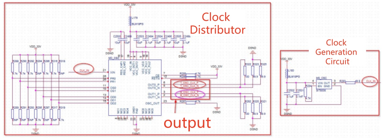
(Clock distributor circuit schematic)
The PCB layout is shown below:
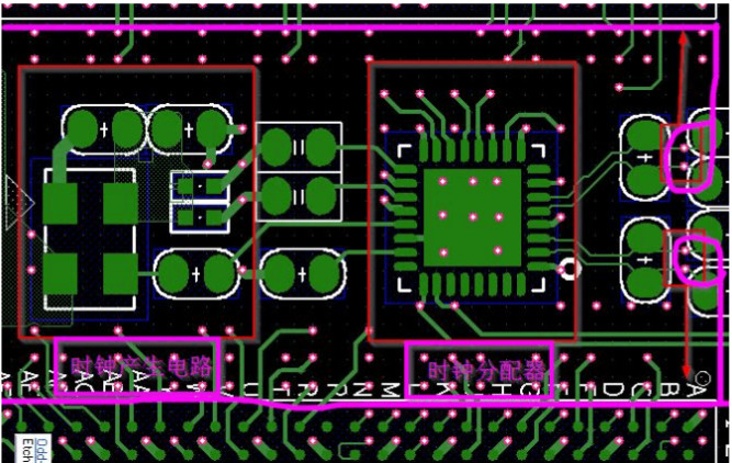
(Clock distributor PCB layout)
Placement and routing guidelines:
A well-designed clock circuit is essential for maintaining stable and reliable operation in electronic systems. Whether using a crystal, an active oscillator, or a clock distributor, careful component placement, short signal paths, proper grounding, and appropriate impedance control all contribute to better clock signal integrity.
By following these PCB clock circuit design guidelines, engineers can reduce noise interference, minimize signal distortion, and improve overall system stability. For projects that require professional PCB layout and routing, PCBWay Design Service can help turn your design requirements into reliable PCB solutions.