 Mila
Oct 20,2026
313
How to Design a Ground Guard Trace in PCB Design
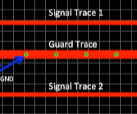
In PCB design, a ground guard trace is a copper trace connected to ground and placed alongside a signal trace or around a sensitive circuit area. It can help reduce unwanted capacitive coupling and el...
| Ranking | Name | Answers |
|---|---|---|
| 1 | PCBWay Team | 2 |


