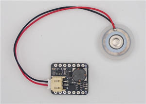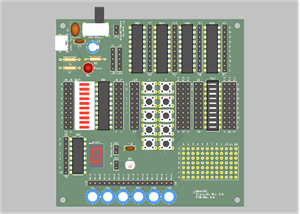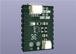
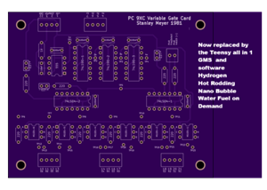
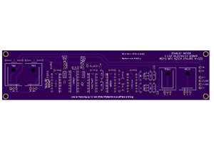
Stanley A Meyer PC9XC Variable Gate Card
Ethan Replication Stanley A Meyer Stanley A Meyer PC9XC Variable Gate Card
Join Us https://www.patreon.com/c/securesupplies
1. Bill of Materials (BOM) — PC-9XC Variable Gate Card
Power & Timing
Qty
Ref
Value
Description
1
U1
NE555
Master timing / gate oscillator
4
U2–U5
74LS90
Decade counters / pulse sequencing
2
U6–U7
74LS04
Inverters / edge conditioning
2
U8–U9
74LS04
Additional buffering
1
LED + R
220 Ω
Gate activity indicator
Logic & Gating
Qty
Ref
Value
Description
2
U10–U11
74LS04
Gate shaping
10
R
220 Ω
Logic current limit
10
C
0.1 µF
Decoupling
—
TP
Test points
Timing analysis
I/O
Qty
Ref
Description
—
Headers
Logic I/O
—
Headers
Channel select
⚠️ No power transistors, no MOSFETs, no BJTs
This is pure logic-level control hardware.
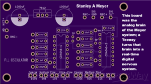
2. What This Board Is (Plain Language)
The PC-9XC Variable Gate Card is a pulse permission controller.
It does NOT:
Create resonance
Generate high power
Drive coils
Switch current
It DOES:
Decide when pulses are allowed through
Gate pulse trains
Sequence outputs
Control dwell and spacing
Think of it as a digital valve, not a pump.
3. Where It Fits in the Stanley Meyer System (Critical Answer)
❌ NOT between cell capacitor and chokes
❌ NOT between transformer and chokes
✅ YES — between PWM / frequency control and power switching
Correct placement:
PLL / Frequency Generator
↓
PC-9XC Variable Gate Card ← (THIS BOARD)
↓
MOSFET / BJT Power Switch
↓
Transformer Primary
↓
Chokes
↓
Cell (Capacitive Load)
👉 It gates the control signal, not the energy path.
4. What Feeds INTO the PC-9XC
Inputs:
Logic-level pulse train
Frequency-controlled signal
Sync or reference pulse
Usually from:
PLL board
Oscillator
Divider
Timing generator
This is information, not power.
5. What Feeds OUT of the PC-9XC
Outputs:
Gated pulse trains
Sequenced logic signals
Enable / disable timing
These outputs go to:
MOSFET gate drivers
BJT base drivers
Transformer primary switches
Again: logic-level only.
6. What It Actually Does Internally
Step-by-step operation:
555 generates a timing envelope
74LS90 counters divide and step pulses
74LS04 inverters sharpen edges
Outputs are selectively enabled
Only allowed pulses continue downstream
This allows:
Burst-mode excitation
Duty-cycle shaping
Controlled pulse windows
Reduced heating
7. Why Meyer Used This Card
In the 1980s–90s:
No fast microcontrollers
No cheap DDS
No software PWM
So Meyer used hardware logic to:
Gate energy
Prevent continuous conduction
Allow dielectric relaxation
Avoid brute-force electrolysis
This card was about rest periods, not power.
8. What Replaces This Board in a Modern (2026) GMS
Short answer:
👉 A Teensy replaces this completely
What the Teensy does instead
PC-9XC Function
Teensy Replacement
Pulse gating
Timer interrupts
Duty shaping
PWM hardware
Sequencing
Software state machine
Enable logic
Firmware flags
Channel select
GPIO mux
One Teensy 4.1 can do everything this board does, plus:
Adaptive control
Feedback loops
Data logging
Safety shutdowns
9. Modern Fast Switching (Downstream, 2026 Tier)
⚠️ Important: MOSFETs do NOT go on this board
They go after it.
Best 2026 switching devices:
Part
Type
Infineon BSC010N04LS
MOSFET
TI CSD18540Q5B
MOSFET
EPC2218
GaN
GS61008T
GaN
Required companion:
High-speed gate driver (UCC27524, TC4427, LM5113)
10. One-Paragraph System Truth (Very Important)
The PC-9XC Variable Gate Card sits between frequency generation and power switching.
It never touches high current and never sits between cell and chokes.
Its purpose was to allow pulses through only when conditions were correct, enforcing rest, spacing, and timing discipline.
In a modern Gas Management System, this function is absorbed entirely into firmware, and the Teensy becomes the true GMS.
Final One-Sentence Answer to Your Question
The PC-9XC Variable Gate Card sat between the PWM/frequency generator and the transformer drive stage, acting as a logic-level pulse gate — not between the cell capacitor and chokes — and today it is completely replaced by a Teensy running gated timing firmware.
If you want next, I can:
Draw a full Meyer GMS signal-flow diagram
Map PC-9XC pins → Teensy GPIO
Write a software gating model
Design a modern MOSFET/GaN driver stage
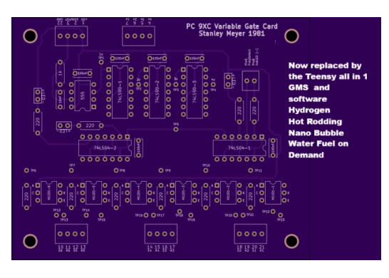
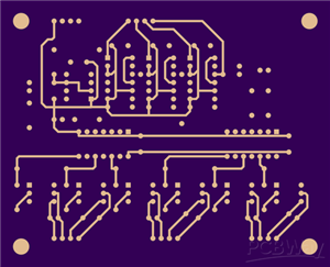
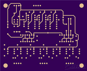
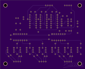
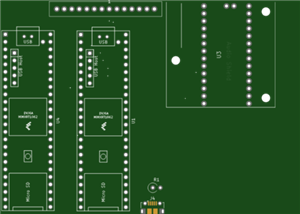
Bill of Materials (BOM) — PC 9XC Variable Gate Card (from the silkscreen you showed)
ICs
1× NE555 (DIP-8) — timing / master gate oscillator
3× 74LS90 (DIP-14) — decade counters / dividers (labeled 74LS90-1/2/3)
2× 74LS04 (DIP-14) — hex inverters / edge cleanup (labeled 74LS04-1/2)
8× H11D1 (DIP-6) — opto-isolators (labeled H11D1-1 … H11D1-8)
Resistors (as labeled on the board)
1× 1 kΩ (near the 555)
1× 10 kΩ (near the 555 area; label appears “10k”)
Many × 220 Ω (clearly repeated near outputs/opto channels; used as LED/opto input current limit and/or logic series resistors)
2× 270 Ω (right side, clearly labeled “270” twice)
1× 2 kΩ (printed above the first counter section)
1× 4 kΩ (printed above the third counter section)
If you want the BOM to be “purchase-ready,” the only missing piece is confirming how many total 220 Ω parts are populated (the silkscreen shows multiple 220 positions). Functionally they’re all the same value.
Capacitors (as labeled)
1× 0.1 µF (100 nF) (near the 555, labeled “100nF”)
3× 0.01 µF (10 nF) (above the 74LS90s, labeled “0.01uF” on each section)
Strongly recommended additions (even if not shown):
0.1 µF decoupling capacitor at each IC (LS logic + counters behave much better with local decoupling)
Connectors / Misc
Pin headers for in/out (top and bottom headers)
Test points TP1…TP23 (for scope timing verification)
LED header marked +LED / − (plus a 220 Ω resistor nearby)
What this board does (plain, accurate)
This is a logic-level “gate window + sequencing + isolation” card.
It does not switch power and it does not sit in the high-current path.
It creates a controlled pulse permission window and distributes/conditions timing, then sends those timing signals through opto-isolators so the next (power) stage can be driven cleanly and safely.
Think: “digital valve for pulses”, not the pump.
How it works (block-by-block)
1) NE555 = master timing / gate-rate source
The 555 generates a clock or timing envelope.
The nearby 1k / 10k + capacitor(s) set the time constant (frequency / gate rate).
2) 74LS90 counters = divide + step the timing
Each 74LS90 takes an input clock and outputs divided counts.
This is how you get:
repeatable burst structures
stepped timing states
selectable duty windows (depending on how the outputs are wired)
3) 74LS04 inverters = sharpen edges + invert as needed
The 74LS04 cleans transitions, restores logic levels, and provides inverted phases where needed.
That improves timing integrity and reduces false triggering downstream.
4) H11D1 opto-isolators = isolation to the next stage
Each H11D1 is basically a light-coupled on/off switch.
Logic drives the opto LED (through 220 Ω resistors).
The opto output side provides an isolated logic-ish signal suitable for feeding:
a gate driver input
a transistor driver stage
another control board
Net effect: clean timing out, less noise injected back into the logic.
Where it fits in the Meyer-style stack (your key question)
✅ It sits between the timing/PWM/control source and the power switching stage
It is in the control signal chain, not the energy chain.
Correct placement:
PLL / Oscillator / Timing source
↓
PC-9XC Variable Gate Card (THIS BOARD)
↓
Power switch stage (MOSFETs / BJTs / gate drivers)
↓
Transformer primary
↓
Chokes
↓
Cell (capacitive load)
❌ It is NOT between:
cell capacitor and chokes (high-voltage/current path)
transformer and chokes (power path)
So your answer is:
Between PWM/timing control and the power switch that drives the transformer/chokes. Not between the cell capacitor and chokes.
Modern improvements (2026 “fastest / best efficiency” direction)
Important: MOSFETs don’t replace anything on this board because this board is logic + isolation.
MOSFETs replace the next-stage power transistors that this board would drive.
A) Replace the H11D1 optos (big upgrade)
H11D1 parts are relatively slow and “soft” compared to modern isolation.
Best modern replacements (by function):
Digital isolators (fast, clean edges): Silicon Labs Si86xx family, ADI ADuM family
Isolated gate drivers (even better if you’re driving FETs): ADI ADuM3223 / ADuM412x, Silicon Labs Si823x, TI ISO5852S (examples of the category)
These give:
sharper edges
less timing skew
higher noise immunity (dv/dt)
more consistent gate signals
B) Replace 74LS logic with modern logic
Swap to:
74HC (CMOS) or 74LVC (faster, lower power, stronger edges)
Benefits:
less power draw
faster transitions
better noise margins (with good layout/decoupling)
C) Replace the 555 + counters with a Teensy (complete modernization)
A Teensy 4.1 can replicate all gating/sequencing in firmware:
programmable gate windows
adjustable duty, burst length, dead-time
closed-loop timing based on feedback
Then you output into:
a proper gate driver
then the MOSFET/GaN stage
D) Best-in-class 2026 switching stage (downstream)
For the actual high-power switching that drives transformer/chokes, typical “top tier” options are:
MOSFET class (efficient, robust):
Infineon OptiMOS families (very low Rds(on), strong switching performance)
TI NexFET families
Nexperia automotive power MOSFET families
GaN class (fastest edges, highest dv/dt):
EPC (EPC2xxx families)
GaN Systems / Infineon GaN families
And pair with a real gate driver (this matters as much as the FET):
high peak gate current
controlled rise/fall (gate resistor + driver strength)
strong UVLO + Miller clamp where needed
Practical action plan (what to do next)
Decide if you want to keep the board “retro-correct” or modernize.
If modernizing:
Replace H11D1 isolation with digital isolators or isolated gate drivers
Move switching to a separate power stage: driver + MOSFET/GaN
If Teensy becomes the “GMS brain”:
Teensy generates the gating windows directly
This board becomes optional (unless you want isolation/headers/test points)
If you tell me what the downstream stage is (transformer primary voltage/current and switching frequency range), I’ll give you a tight, parts-specific recommendation for:
the exact MOSFET vs GaN choice
the exact gate driver choice
the protection parts (TVS, snubbers, diodes) that make it survive and stay fast
Stanley A Meyer PC9XC Variable Gate Card
*PCBWay community is a sharing platform. We are not responsible for any design issues and parameter issues (board thickness, surface finish, etc.) you choose.


Raspberry Pi 5 7 Inch Touch Screen IPS 1024x600 HD LCD HDMI-compatible Display for RPI 4B 3B+ OPI 5 AIDA64 PC Secondary Screen(Without Speaker)
BUY NOW

- Comments(2)
- Likes(0)
More by Daniel Donatelli
-
 Stanley A Meyer VIC Voltage intensifier circuit transformer board v1.8 updated jan 11 2021
Stanley A Meyer VIC Voltage intensifier transformer board Join Support help change the World https:/...
Stanley A Meyer VIC Voltage intensifier circuit transformer board v1.8 updated jan 11 2021
Stanley A Meyer VIC Voltage intensifier transformer board Join Support help change the World https:/...
-
 STANLEY A MEYER LES BANKI AUTO START AUTO WATER FUEL REFILL
Join Support help change the World https:...
STANLEY A MEYER LES BANKI AUTO START AUTO WATER FUEL REFILL
STANLEY A MEYER LES BANKI AUTO START AUTO WATER FUEL REFILLJoin Support help change the World https:...
-
 Stanley A Meyer Gated Pulse Frequency Generator K3 with DB 37 updated 060622
Stanley A Meyer Gated Pulse Frequency Generator K3 with DB 37 to suit matrix vic main board Join Sup...
Stanley A Meyer Gated Pulse Frequency Generator K3 with DB 37 updated 060622
Stanley A Meyer Gated Pulse Frequency Generator K3 with DB 37 to suit matrix vic main board Join Sup...
-
 Stanley A Meyer K2 Variable Pulse Frequency Generator GMS Vic Matrix PCB Gerber
Stanley A Meyer K2 Variable Pulse Frequency Generator GMS Vic Matrix PCBGerberJoin Support help chan...
Stanley A Meyer K2 Variable Pulse Frequency Generator GMS Vic Matrix PCB Gerber
Stanley A Meyer K2 Variable Pulse Frequency Generator GMS Vic Matrix PCBGerberJoin Support help chan...
-
 Hyduino Stim Stimulator circuit board Ms EMS ECU
Join Support help change the World https://www.patre...
Hyduino Stim Stimulator circuit board Ms EMS ECU
Hyduino Stim Stimulator circuit board Ms EMS ECUJoin Support help change the World https://www.patre...
-
 Stanley A Meyer VIC Daughter Board Driver Transistor Circuit board Version 1
 Updated 28th Sept 2021 ...
Stanley A Meyer VIC Daughter Board Driver Transistor Circuit board Version 1
Stanley A Meyer VIC Daughter Board Driver Transistor Circuit board Version 1 Updated 28th Sept 2021 ...
-
 Stanley A Meyer VIC Daughter Board Driver USed with Variac EEC eleectron eextrract & chokes
Stanley A Meyer VIC Daughter Board Driver USed with Variac EEC eleectron extrract & chokes can d...
Stanley A Meyer VIC Daughter Board Driver USed with Variac EEC eleectron eextrract & chokes
Stanley A Meyer VIC Daughter Board Driver USed with Variac EEC eleectron extrract & chokes can d...
-
 Stanley A Meyer Taking Gas Management Warning Board Stans Voice
 Who Wants to Clone Stans Voice and M...
Stanley A Meyer Taking Gas Management Warning Board Stans Voice
Stanley A Meyer Taking Gas Management Warning Board Stans Voice Who Wants to Clone Stans Voice and M...
-
 Stanley A Meyer Stack Resonant Cavity
Dynamysthesis: Force-Dominant Energy Release via Charge-Separated Fuel Collapse1. Definition of Dyna...
Stanley A Meyer Stack Resonant Cavity
Dynamysthesis: Force-Dominant Energy Release via Charge-Separated Fuel Collapse1. Definition of Dyna...
-
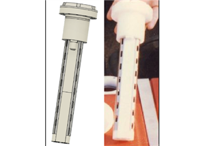
 Stanley A Myer nano bubble water fuel 9 TUBE CELL Modern 3d Print
Join Us https://www.patreon.com/c/s...
Stanley A Myer nano bubble water fuel 9 TUBE CELL Modern 3d Print
Stanley A Myer nano bubble water fuel 9 TUBE CELL Modern 3d PrintJoin Us https://www.patreon.com/c/s...
-
 Stanley A Meyer Nano Bubble Water Fuel Tank Steam Defrost Resonator
Stanley A. Meyer Nano-Bubble Water Fuel Tank Steam Defrost ResonatorTechnical DescriptionJoin Us htt...
Stanley A Meyer Nano Bubble Water Fuel Tank Steam Defrost Resonator
Stanley A. Meyer Nano-Bubble Water Fuel Tank Steam Defrost ResonatorTechnical DescriptionJoin Us htt...
-
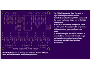 Stanley A Meyer PC9XE Sequential Gate Circuit
Ethan Replication Stanley A Meyer PC9XE Sequential Gate Circuit 1. Where This Board Fits in the Stan...
Stanley A Meyer PC9XE Sequential Gate Circuit
Ethan Replication Stanley A Meyer PC9XE Sequential Gate Circuit 1. Where This Board Fits in the Stan...
-
 Stanley A Meyer PC9XC Variable Gate Card
Ethan Replication Stanley A Meyer Stanley A Meyer PC9XC Variable Gate CardJoin Us https://www.patreo...
Stanley A Meyer PC9XC Variable Gate Card
Ethan Replication Stanley A Meyer Stanley A Meyer PC9XC Variable Gate CardJoin Us https://www.patreo...
-
 Stanley A Meyer PLL Gated Frequency Generator
Ethan Replication bom notes and advancing it Stanley A Meyer PLL Gated Frequency Generator2. Wher...
Stanley A Meyer PLL Gated Frequency Generator
Ethan Replication bom notes and advancing it Stanley A Meyer PLL Gated Frequency Generator2. Wher...
-
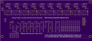 Stanley A Meyer EPG Magnetic Spin Gerbers MUlt i Trigger VIc or Coils
You’re looking at a multi-channel sequential magnetic driver. This is not a simple oscillator board ...
Stanley A Meyer EPG Magnetic Spin Gerbers MUlt i Trigger VIc or Coils
You’re looking at a multi-channel sequential magnetic driver. This is not a simple oscillator board ...
-
 Stanley A Meyer Steam Resonator PCB
1. Bill of Materials (BOM)Based on silkscreen labels visible on the PCB. Values are conservative and...
Stanley A Meyer Steam Resonator PCB
1. Bill of Materials (BOM)Based on silkscreen labels visible on the PCB. Values are conservative and...
-
 U-Core Bobbin for VIC Transformer | 8XA Stanley A. Meyer Style | Ferrite U126x91x20 | High-Voltage Experimental Coil Former
Stanley A. Meyer U-Core Bobbin – 8XA ConfigurationFerrite U-Core Bobbin for VIC / Water Fuel Cell Re...
U-Core Bobbin for VIC Transformer | 8XA Stanley A. Meyer Style | Ferrite U126x91x20 | High-Voltage Experimental Coil Former
Stanley A. Meyer U-Core Bobbin – 8XA ConfigurationFerrite U-Core Bobbin for VIC / Water Fuel Cell Re...
-
 Nano Second Laser Diode Driver STANLEY a MEYER Nano Bubble Water Fuel
 # Avalanche Laser Diode Driver...
Nano Second Laser Diode Driver STANLEY a MEYER Nano Bubble Water Fuel
Nano Second Laser Diode Driver STANLEY a MEYER Nano Bubble Water Fuel # Avalanche Laser Diode Driver...
-
Programmable Mist Maker - XIAO / QT PY Extension
867 1 0 -
RadioHAT - Raspberry Pi radio development platform
696 0 2 -
-
-
-
-
ARPS-2 – Arduino-Compatible Robot Project Shield for Arduino UNO
3166 0 6 -
A Compact Charging Breakout Board For Waveshare ESP32-C3
3782 3 8 -
AI-driven LoRa & LLM-enabled Kiosk & Food Delivery System
4125 2 2