 Mila
Dec 30,2025
3288
Mila
Dec 30,2025
3288
RF PCB Design Guidelines: Key Considerations for High-Frequency Circuits
In recent years, the rapid growth of Bluetooth devices, wireless local area networks (WLAN), and mobile communication systems has driven increasing attention to RF circuit design techniques. From past...
Mila
Dec 20,2025
4398
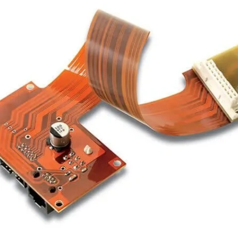
Flex PCB Bending Area Design Guidelines: How to Prevent Trace Cracking and Failure
Flexible circuit design involves many challenges. Flexible PCBs must overcome copper work hardening and fatigue, maintain adequate flexibility, and prevent tearing of the FPC substrate. In Flexible PC...

 William Harter
Dec 06,2025
1507
William Harter
Dec 06,2025
1507
Tip for placing decoupling capictors
Here’s a helpful suggestion for placing decoupling capacitors in KiCad. When assigning references to decoupling capacitors, use the format C#-U#. For example, if IC U1 is paired with capacitor C3 as i...
Mila
Nov 28,2025
2313
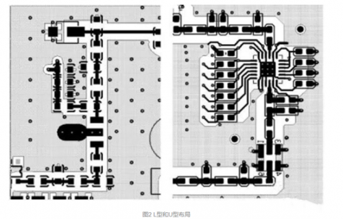
Essential Tips for Compact PCB Designs: Practical Layout Strategies for Limited Space
As electronic devices continue to shrink in size, their internal circuits must also become smaller. Product miniaturization has become a strong industry trend, creating new challenges for engineers wo...

Mila
Nov 24,2025
23759
ESP32 vs ESP32-S3: Key Differences, Performance Comparison, and PCB Design Considerations
Since the ESP32 series entered the market, it has reshaped the landscape of embedded development and the Internet of Things. The ESP32 microcontroller became widely adopted thanks to its exceptional p...
Mila
Nov 07,2025
3755
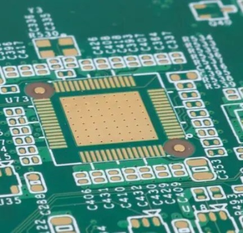
PCB Layout Design Guidelines: Placement and Routing
Overview of PCB Layout and RoutingIn PCB design, layout is a critical stage that directly determines the quality of the routing. A well-organized layout ensures efficient signal paths and reliable pow...
Mila
Nov 05,2025
2137
What Is Test Firmware: Key Differences Between Test Firmware and Embedded Software
In hardware design process, especially for complex projects, we often recommend developing dedicated testing firmware to perform comprehensive hardware validation. In this article, we will explain the...
Mila
Oct 27,2025
4365
High Current Trace Design Considerations in PCB Layout
High Current PCB is a special type of circuit board designed to carry large amounts of current. Compared to ordinary PCBs, it can handle more power, which makes it indispensable in many high-power app...
Mila
Oct 21,2025
5551
Power and Ground Plane Design Considerations in PCB Layout
The power and ground planes form the backbone of a stable and efficient PCB design. The ground plane acts as a common reference point for all electrical signals and provides a low-impedance return pat...
Mila
Oct 14,2025
4668
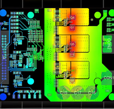
Thermal Management Design Considerations in PCB Layout
Thermal management in modern PCB design is a critical factor that directly impacts product performance, reliability, and lifespan.As electronic products continue to become more compact and integrate m...
Mila
Sep 25,2025
2662
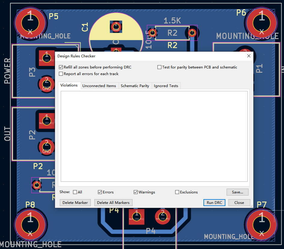
How DRC Improves PCB Layout Reliability
DRC (Design Rule Check) is an essential step in PCB Layout design that ensures your layout complies with the manufacturing capabilities of the PCB fabrication house. Performing DRC before sending your...
Mila
Sep 17,2025
5645
EMC Design Guidelines in PCB Layout Design
Understanding EMI, EMS, and EMC in PCB DesignEMI (Electromagnetic Interference) refers to the harmful electromagnetic noise emitted by electronic products during operation, which can interfere with ot...
Mila
Sep 16,2025
3924
PCB Layout Design Process from Schematic to Manufacturing
PCB layout is the process of converting a circuit schematic into a manufacturable PCB design. A high-quality PCB layout ensures the functionality, reliability, and performance of the final product whi...
Mila
Sep 08,2025
2237
How PCB Design Decisions Impact Manufacturing Cost
PCB Design directly affects Manufacturing Cost—the more complex the PCB Design, the higher the Manufacturing Cost. Therefore, when submitting design requirements, customers can provide a target cost r...
Mila
Sep 05,2025
1908
PCB Design Process from Concept to Manufacturing
Every step in the PCB design process is crucial to the success of the final product. A rigorous and efficient PCB design workflow ensures optimal functionality, performance, reliability, and cost-effe...
Anson
Sep 03,2025
1139
Why Professional PCB Design is Worth the Investment
Many customers feel that PCB design fees are high compared to manufacturing costs, but in reality, professional design is the foundation of a successful electronic product. An investment in quality de...
Mila
Sep 03,2025
1538
From Design to Production: Discounts and Advantages for Bulk Orders
Once your design project is completed, you can place a bulk production order directly through PCBWay. We will handle the entire process from design to manufacturing, providing a one-stop service....
Anson
Jun 27,2025
5068
What Detailed Information Is Needed for Electronic Design
PCBWay offers professional electronic design services. This article outlines the key information required for successful electronic design1. For PCB design, the following requirements need to be provi...

 Zaoui Mohamed el amine
Mar 26,2025
4595
Zaoui Mohamed el amine
Mar 26,2025
4595
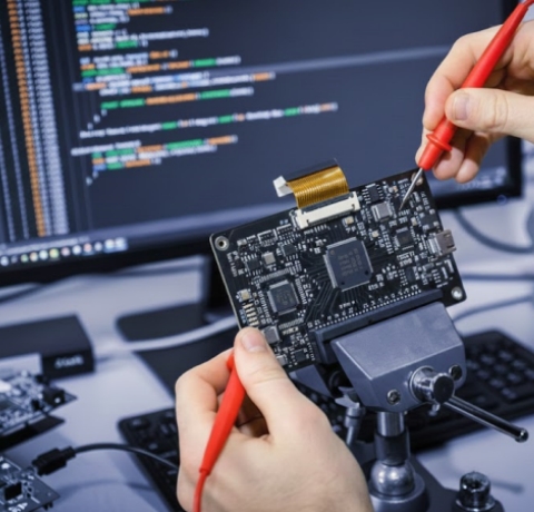
Teleoperated Robot PCB
In the realm of robotics, teleoperated robots stand as a marvel of modern engineering, combining automation with human control for various tasks that require precision, flexibility, and adaptability. ...

PCBWay
Feb 28,2025
6642
Considerations for High-Power PCB Design
In modern electronic devices, high-power power supplies provide stable and reliable power for servers, electric vehicle chargers, and various industrial equipment, ensuring that the devices operate pr...
| Ranking | Name | Answers |
|---|---|---|
| 1 | Avaq Semiconductor | 1 |


