Here is a way of panelizing PCBs with tabs and mouse bites in Kicad shared by Sayanee Basu.

The example KiCad project is iCEBreaker FPGA
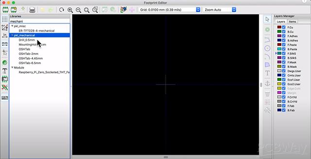
1.Panelization footprint
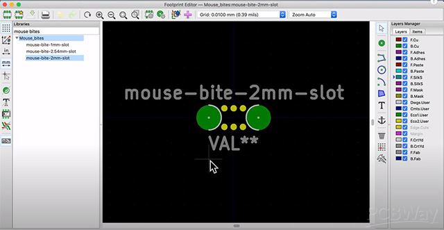
Open up the footprint editor, decide which mouse bite footprint to use
Footprint by Piotr Esden-Tempski
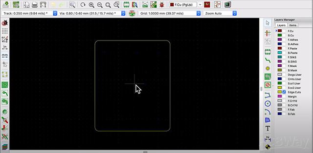
2.Original board
1)Grid size
choose the slot and grid size that is applicable to the mouse bite footprint.

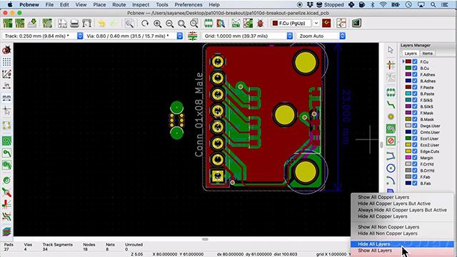
>>Hide layers, just turn on the edge cut layer
Ensure that the cut layer is kind of drawn in the grid size you have chosen, so that it will be easy for us to repeat this component as an array when we panelize the entire board.
>>Choose “E”, change it to comments or drawings user layer

>>So in the drawings(dwgs) user layer, you will see the same edge cuts

>>Save the board
2)Edge cuts layer
Open pcbnew app

>>Ensure the grid size. Append board, go back to the layout file for the single board and save it

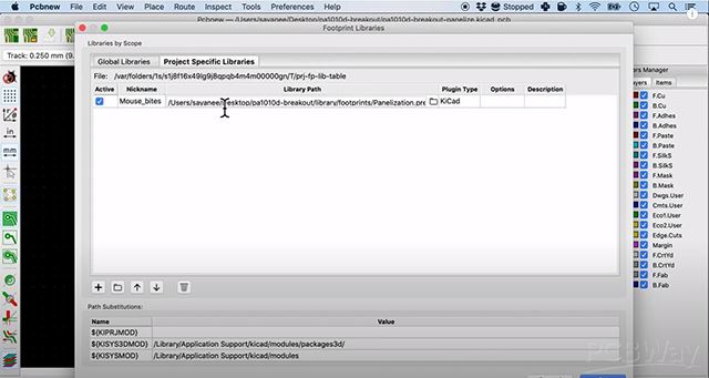
>>Add the footprint for the mouse bite and ensure the mouse bite footprint is part of the library.
>>Search for the mouse bite to ensure

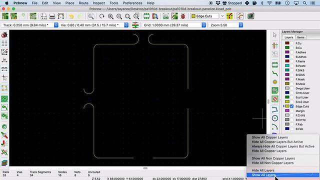
>>Hide all layer, just choose the drawings layer and the edge cuts layer for the purpose of clarity.

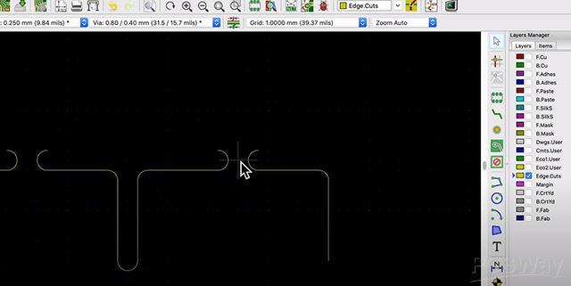
>>Choose the edge cut layer and the line tool “add graphic lines”, drawing over the comments layer as a guide line.

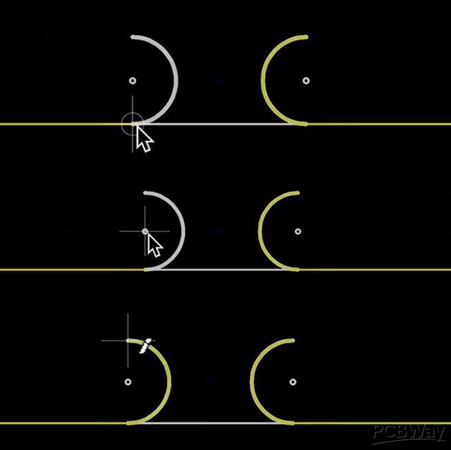
>>For the arcs, click once in the middle of the circle,once at the outer diameter and the arcs in counterclockwise
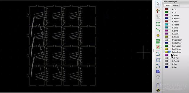
>>Looks like the edge cuts layer is ready to be repeated, turn on all the layers.
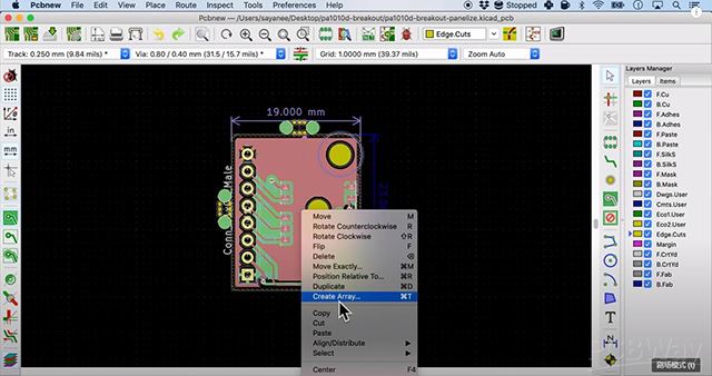
>>Create array (take the board length and plus it)

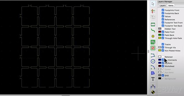
>>Hide all layers, just enable the edge cuts layer, disable the ratsnest
>>Close all the edge cuts layer especially at the boundaries
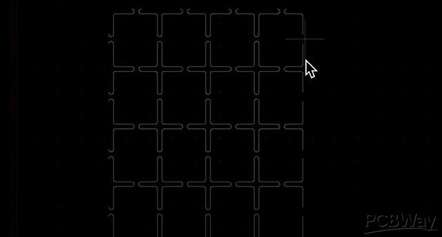
>>Delete away the mouse bites at the edges

>>Delete tiny little arcs
>>Close up all the edge cuts layer using graphic line

>>Do the DRC check

>>Show all the layers

Thanks for Sayanee Basu's sharing.
More interesting video on Sayanee Basu's Youtube Channel.


