
Note:Now you can place order directly by PCBWay Plugin for KiCad
Hello everybody, today we are going to have an interesting class on electronic design automation (EDA) software. Our main focus will be on KiCAD as an EDA tool. This is one of the very important tools in the design of electronics especially printed circuit boards. It is, therefore, very important for students and designers to familiarize themselves with such a helpful tool. Although we have so many EDA software such as Proteus, Eagles, Altium, Easydraw, Fritzing, and many others, our focus today will mainly be on KiCAD.
KiCAD is an EDA software that was first introduced to the market in 1992 by Jean-Pierre Charras. It has undergone various changes since that time and today it is under the management of the KiCAD Development Team.
Let us discuss why a good designer should learn and use KiCAD.
Have you ever of owning your projects? If yes is your answer, then KiCAD takes care of that. Open-source software means the designer is allowed to own the data. KiCAD allows anyone to use and download the data on their computers. This is the best software for developers who want to do heavy and new designs anytime.
Why spend is money buying software while you can own one for free? KiCAD is freely available for anybody who wants to download and use it.
This is one EDA software with so many important features such as length matching, interactive routing, and differential routing. Also, the software being open source you can add external software such as autoroute through add-ons.
You can use KiCAD anywhere whether you are using Windows, Linux, or IOS.
KiCAD has no limited version. It has no medium or professional. KiCAD is just one.

When you want to start with KiCAD, the first thing you have to do is download and install it.

Let us start with the navigation bar;

1. File.
This is where the opening of the new or old project is done. It is the first command to use anytime you open KiCAD. Two very important commands for beginners are NEW or OPEN PROJECT.

When you click new, you will be creating a new project for the first time and when you hit on the open project, it means you want to navigate through an existing project saved on your computer.


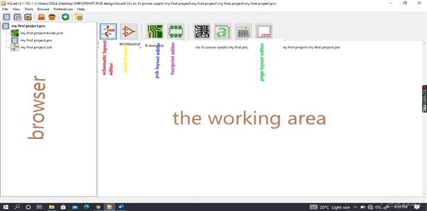
- Browser shows the proceedings of your design. Anything you add to your design is shown on the browser.
- Schematic layout editor is where you edit or create your schematic.
- Symbol editor is where you edit the symbol of the components you have placed if need be.
- Footprint editor is where you edit your footprints. The footprint is a pattern that represents an electronic element that is to be soldered on the PCB board.
- Page layout editor is where you edit your working area.
- The working area is where now you do the actual drawing of your schematics.
We cannot discuss KiCAD and fail to list important hot keyboard shortcuts. These shortcuts are significant because they will impact greatly how fast you will be doing your design.
These are the hotkeys used during the design of the schematic components in KiCAD


the left column. When you filter, you will have the right footprints on the right column. So hoover over-filtered footprints on the right and when you get the right footprint just double left click to add it to your components at the center column.

Note that my rectifier and transformer have no footprints.
This is what describes the connection between electrical components before going to the PCB layout environment.

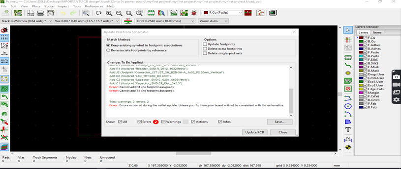
This is another significant step in the use of KiCAD. This is where the actual conversion of the schematic into the PCB takes place. It has several steps and they shall be discussed below.
To go to the 3D design environment, click on the icon labeled Run PCBnew to layout the PCB board. We shall have a window shown below.

At this PCB layout window, the first thing is to place the netlist that we saved earlier. Now here you get to know why we needed netlist generated.

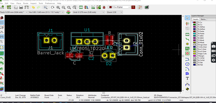
Now let us arrange the components in preparation for routing. You can zoom your design to see the component well.

BOM files
GERBER files.
Pick and place files
Drill files.

And this makes the end of our introduction to KiCAD class. Thank you for following and all the best as you begin your design with KiCAD.


