PCB Prototype the Easy Way

Full feature custom PCB prototype service.

Help Center
Sending a message
9:00 - 23:00, Mon.- Sun. (GMT+8)
Service hotlines
+86 571 8531 7532

9:00 - 18:00, Mon.- Fri. (GMT+8)

9:00 - 12:00, Sat. (GMT+8)

(Except Chinese public holidays)

Unlock New Potential,Product Categories:

  • Multi-layer PCB (6-40 layers)
  • Rigid-Flex PCB
  • HDI PCB
  • High Frequency / Microwave
  • Metal Core / Metal Base
  • High Speed Signal Transmission
  • Impedance control PCB
  • Buried blind pore plate
  • Blue rubber plate
  • Carbon oil plate

Items

Application

  • Engineering
  • Production
  • Quantity
  • Material
  • Ink,Soldermasks
  • drilling
  • plating
  • Soldermask offset
  • Dimensional
    deviation
  • Warping angle
  • Test method
  • Glass transition ℃
  • Package
  • Inspection report
  • Standard
  • Etched line
  • Cleanliness
  • Certification

Advanced PCB

HIGH-END,COMPLEX

IDEAL IF YOU NEED A HIGH-END, COMPLEX PCBS

Industrial equipments, instrumentation, automotive electronics, communication equipments, etc. Finished products require high reliability and stable quality for users

  • Senior engineer (one file/6 hours)
  • individual working panel
  • ≥1 piece
  • Shengyi,Rogers,Arlon,Isola,Omega,Nelco,3M etc.
    Meet IPC4101 class B/L
  • Rohm&Haas,TAIYO,Kuangshun,Meet IPC-SM-840 class T
  • Min Mechanical Hole Size 0.15mm,Laser hole 0.1mm
  • PTH (Hole copper thickness≥20um),IPC 3(25um)
  • ±2mil
  • ±0.13mm
  • 0.75%
  • A.O.I,Kelvin Four-terminal sensing,Microsection Inspection,Solderability Test,Impedance Test...
  • >140℃
  • Humidity indicator cards
  • Inspection report
  • IPC Class 2,IPC Class 3,Automotive Standard,Customer Standard
  • Forbid to repair tracks(IPC 3,Automotive,Customer Standard)
  • Cleanliness requirements beyond those of IPC
  • UL,ISO9001:2008,ISO14001:2004,ISO/TS16949:2009,RoHS etc.

Standard PCB

inexpensive , FAST

IDEAL IF YOU NEED A inexpensive, QUICK-TURN PCB

Children's toys, small appliances, home lighting, functional testing, electronic enthusiasts, etc. Suitable for users whose prices are core competitiveness

  • mid-level engineer (5 files/hours)
  • mixed working panel
  • 5,10,15,20,25...pieces
  • KB(kingboard)/GDM(goldenmax)
    Meet IPC4101 class B/L
  • TAIYO,Kuangshun,Meet IPC-SM-840 class T
  • Min Mechanical Hole Size 0.2mm
  • PTH(Hole copper thickness≥18um)
  • ±3mil
  • ±0.2mm
  • 1%
  • A.O.I.,Fly Probe Testing
  • >130℃
  • None
  • None
  • IPC Class 2
  • -
  • Meet IPC standards
  • UL,ISO9001:2015,RoHS etc.

Factory Scale

PCBWay's high-quality PCB R&D and manufacturing base (including the cooperative factory) is located in Shenzhen, China, with a plant area of 80,000 square meters and professional technicians accounting for 35% of the total number. It specializes in high-end prototypes, quick turn and small volume hardware designing and manufacturing services.Such aspects should be borne in mind when comparing PCB prices. Reliability and a guaranteed/long life cycle involve an initially higher outlay, but will pay for themselves in the long run.

Laser Drilling

Laser Drilling

Laser Drilling

Minimum aperture up to 0.1mm for high-density interconnection (HDI) build-up multi-layer PCB, with electrical conduction between wirings on each layer controlled through interlayer vias. Currently laser drilling machines are extensively applied in processing of the Interlayer via-holes.

PCB Via Hole Plugging

PCB Via Hole Plugging

PCB Via Hole Plugging

Via Fill is a special PCB manufacturing technique used to selectively and completely close via holes with epoxy. There are many instances in which a PCB designer might want to have a via filled. Some key benefits are:
More reliable surface mounts
Increased assembly yields
Improved reliability by decreasing the probability of trapped air or liquids.

Plating Through Holes

Plating Through Holes

Plating Through Holes

Real-time monitoring of chemical quality in copper plating sinks. The aim of electroless copper is to plate a conductive layer through a hole or into a blind microvia.

Vacuum Etching

Vacuum Etching

Vacuum Etching

Using the vacuum etching technology to make sure that both surfaces of the board are very uniform. it produces a straighter conductor profile, allowing the resulting plate to more accurately match the wiring requirements.

High-quality PCBs Showcase

More To Love,View More >

Application Area

Advanced PCB is widely used in communications, industrial control, computer applications, medical, test equipment and other fields. The core competitiveness: leading technology, high quality, high precision rate, expedited delivery, consultative customer service, and optimal cost performance. With ISO9001, ISO14001, TS16949, UL, RoHS certification.

  • Telecom

    5G/4G, wireless communication, digital TV, mobile phone, fiber optic communication, communication equipment, radio frequency, Bluetooth, radio

  • ELECTRONIC INDUSTRY PCBS

    The consumer electronics industry demands high performance technology to be complex and compact at the same time.
    Industrial instrumentation, sensors, robots, automation, motors, internet of things

  • MEDICAL INDUSTRY PCBS

    The medical field requires a vast level of technology with extreme reliability and long term life cycles.
    3D printing, mobile medical, internet +, medical equipment, wearable, telemedicine

  • AUTOMOTIVE INDUSTRY PCBS

    The automobile industry must have circuit boards that are extremely reliable with an emphasis on safety.
    Electric vehicles, automotive electronics, new energy vehicles, car networking, automotive electronics, body electronics, powertrain, automotive safety

Why PCBWay Advanced High-quality PCB

Advanced Technology +
1. Up to 64 layer processing technology, the minimum trace and space is 2.5 / 2.5mil, the highest ratio of board thickness and hole diameter is 16:1.
2. Long and short gold finger processing technology and high-density trace’s precision control to meet the design requirements of photoelectric communication products.
3. High-precision back-drilling technology to reduce the equivalent series inductance of vias and in case to meet the product’s integrity requirements of signal transmission;
4. Advanced metal-based and ultra-thick copper manufacturing process to meet the high heat dissipation requirements of power products.
5. High-precision mechanical and laser depth control technology to achieve multi-level step groove product’s structure and meet the different levels of assembly requirements.
6. The mature mixed pressure process realizes the mixing of FR-4 and high-frequency materials, and saves the material cost for customers under the premise of achieving the high-frequency performance of the products.
7. Advanced Anti-CAF process technology greatly improves the reliability and service life of PCB products.
8. Advanced buried capacitor and buried resistor technology greatly improve the performance of PCB products.
9. Advanced inner layer exposed technology meets the information transmission requirements of high frequency circuits.

FPC 1. The technical team consists of dozens of engineers who have more than 10 years of FPC processing experience. New equipment are introduced in millions of dollars yearly to continuously improve the process manufacturing capability.
FPC 2. The highest 16-layer Rigid-flex PCB processing technology, the minimum trace and space is 2/2mil, the minimum via is 4mil.
FPC 3. Rich experience in manufacturing FPC products for medical and consumer electronics.
Strict Quality Control+
1. UL certification.
2. ISO9001:2008 quality certification.
3. ISO/TS1694:2009 certification.
4. GJB9001B military standard certification.We do not manufacture and don't accept PCB products such as various weapons and equipment and military equipment.
5. Enterprise standards like SIEMENS and GREE.
6. Strictly manage the processing of customized products according to IPC6012 II /III/customer standard/enterprise internal standard.
7. Strict management for customer information confidentiality.
Advanced Processing And Testing Equipment+
1. Orbotech AOI (automatic optical inspection) machine imported from Israel for detecting high-precision circuits.
2. The high-precision impedance tester imported from the United States meets the impedance test requirement.
3. PLASMA plasma processing equipment, used for hole wall degumming of PTFE, ceramic fillers and other high-frequency material.
4. Ende CNC drilling machine imported from Taiwan for back drilling and deep hole control.
5. Orbotech LDI machine (laser direct imaging) imported from Israel for graphic transfer of high-precision circuits.
6. Ende CNC numerical control molding machine imported from Taiwan, used for deep-groove milling of stepped groove structure products.
7. BURKLE lamination imported from Germany for multi-layer boards pressing.
8. Vacuum resin plugging machine for hole plug in BGA panel of ultra high-precision circuits.
9. Ion staining tester, anti-stripping strength tester, hole copper tester, secondary element tester, copper thickness tester and other reliability testing equipment to ensure product quality.
High-quality Raw Materials+
1. PCB substrate materials: Select the top brands in the industry: Shengyi, ROGERS, ARLON, TACONIC, 3M, Omega, etc.
2. Auxiliary materials: Rohm and Haas electroplating syrup, Hitachi dry film, Taiyo ink, Noda resin, etc.
Fast And Efficient Service Capabilities+
1. Efficient service
1 minute to respond to customers, 1H to reply results, 1 day to solve problems, 1 week to complete service.
2. Fast delivery (work day,China Time Zone(GMT+8))

Layers

Build Time(H:hours)

2layers

18H+1days

4layers

24H+1days

6-8layers

48H+1days

10-12layers

72H+1days

14-22layers

96H+1days

24layers

120H+1days

Have Questions?

If you have any questions or need any further information, please feel free to contact your dedicated customer service.

Send message
placeholder for eslint

Hear from Our Customers

<
>
Takafumi Miyoshi
Company: ***
Industry: Electronics
Massimo
Company: ***
Industry: servo
Stephen Smith
Company: ***
Industry: radio
Mike Bach
Company: ***
Industry: Arduino
Sharipov Sergey Yul'evich
Company: ***
Industry: engine preheater

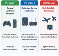
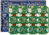
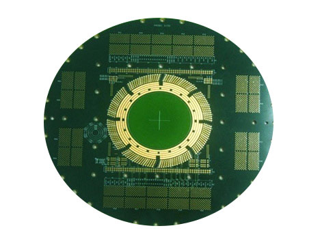
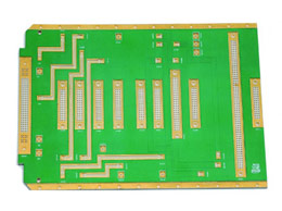
This is my private project of SDR (one microprocessor, FPGA and digital downconverter). My first cooperation with PCBWay is really happy experience. Very quick review by professional, and on-time production. Most of traces are dense as design rule limit (6mil/6mil), and layout has BGA pads with vias, product quality is very satisfying. I'll definitely order again.

The project is a simple Remote Pet Surveillance system based on RPi. This pcb is a RPi shield board to receive some input signals and drive some DC motors and a servo. The PCWay constantly confirms that its production is always top quality and their production price and delivery time is unbeatable. Thank you.

Project is an Allstar node for ham radio with a 6 pin DIN connector. Included installing all surface mount parts. Boards look great. Yolanda was super helpful in fixing a mistake I made in the BOM.

Door Control Module v2.0 uses an Arduino Nano to control I/O. Inputs come via serial from other Modules, Window/Mirror Switches via resistance, and SPI. Outputs are over serial to other modules, SPI to the TLE94108 to control mirror adjustment and folding, and to a Pololu G2 motor driver to control window functions. From initial order over the website, to submitting gerbers, drill files, alternate parts, etc, Angell was super helpful. Production time was quicker than estimated and boards came out perfect. Drill holes are centered, all through hole parts fit perfectly, and the finished product is beautiful and extremely high quality. And the price!!!! It's incredible the quality you get for such an amazing price.

I made an order for the first time. Everything is much easier than it seems at the beginning. I look forward to continuing. High quality products. Soldering point is excellent. if you want to understand how great everything is - just place an order (not an advertisement). Now my car will be the happiest! :)