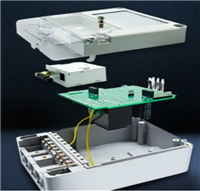
The definition of high-frequency PCB may vary in the industry, but generally, a high-frequency PCB refers to a printed circuit board with a frequency above 1 GHz. High-frequency PCBs have stringent requirements for various physical properties, precision, and technical parameters. They are commonly used in radar systems, military equipment, aerospace applications, and other fields. When designing high-frequency PCBs, designers must consider several parameters to meet the signal requirements of specific high-frequency applications, including the dielectric constant (Dk), dissipation factor (Df), coefficient of thermal expansion (CTE), and thermal conductivity.
Characteristics of High-frequency PCB
Low dielectric constant (Dk): Reduces signal delay and improves frequency transmission. In most cases, a lower Dk is preferred as high Dk can cause signal transmission delays.
Low loss factor (Df): Minimizes signal loss and improves signal transmission quality. A lower Df results in lower signal loss.
Coefficient of thermal expansion (CTE): This should ideally match that of the copper foil to prevent separation during thermal fluctuations.
Low water absorption: High water absorption can affect Dk and Df, especially in humid environments.
Good thermal resistance, chemical resistance, impact resistance, and peel strength are essential.

High-frequency PCB Design Considerations
Routing Method
In high-frequency PCB routing design, if bending is required, one can choose between a 45-degree bend or a curved turn. This approach reduces the chances of high-frequency signal emission and coupling.

Routing Length
In high-frequency PCB routing during PCB design, shorter routing lengths are preferred, and shorter distances between parallel traces are desirable. The radiation intensity of a signal is directly related to the length of the signal trace. Longer high-frequency signal traces result in increased coupling with other components. That's why clock signals, DDR, USB, Gigabit Ethernet, and HDMI prefer shorter routing lengths.
Number of Vias
In high-frequency PCB routing during PCB design, fewer vias are preferred. Each via introduces approximately 0.5 pF of distributed capacitance. Reducing the number of vias can improve signal speed and reduce the likelihood of data errors. Via stubs introduce impedance discontinuities that can lead to signal integrity issues.
Avoiding Crosstalk
When routing high-frequency circuits, it is important to consider the "crosstalk" introduced by closely parallel signal traces. Crosstalk refers to the coupling phenomenon between signal lines that are not directly connected. As high-frequency signals are transmitted in the form of electromagnetic waves along transmission lines, the signal lines act as antennas, emitting electromagnetic field energy around the transmission line. The undesired noise signals generated due to the mutual coupling of electromagnetic fields between signals are referred to as crosstalk.
The parameters of PCB layer stack-up, spacing between signal lines, electrical characteristics of the driver and receiver ends, and termination methods of signal lines all have an impact on crosstalk. Therefore, to reduce crosstalk in high-frequency signal routing, the following points should be considered:
If the layout space allows, inserting a ground wire or ground plane between two lines with significant crosstalk can provide isolation and reduce crosstalk.
When there is a time-varying electromagnetic field in the space surrounding the signal lines, if parallel distribution cannot be avoided, placing a large area of "ground" on the opposite side of the parallel signal lines can greatly reduce interference.
Increase the spacing between adjacent signal lines and reduce the parallel length of the signal lines, if permitted by the layout space. Clock lines should ideally be perpendicular to critical signal lines rather than parallel.
If parallel traces within the same layer are nearly unavoidable, in adjacent layers, the routing directions of the traces must be mutually perpendicular.
In digital circuits, clock signals typically have fast edge transitions and significant external crosstalk. Therefore, in design, clock lines should be surrounded by ground lines and multiple ground via holes should be used to reduce distributed capacitance and thereby reduce crosstalk.
For high-frequency clock signals, it is advisable to use low-voltage differential clock signals with a grounded enclosure. Attention should be paid to the integrity of the ground via holes.
Unused input terminals should not be left floating but should be grounded or connected to the power supply (which serves as the ground in high-frequency signal circuits) because floating lines can act as emission antennas. Grounding can suppress emissions. In practice, this method has proven to be effective in eliminating crosstalk.
Add High-frequency Decoupling Capacitors to the Power Supply Pins of Integrated Circuit Chips
Each integrated circuit (IC) chip should have a high-frequency decoupling capacitor placed near its power supply pins. Adding high-frequency decoupling capacitors to the power supply pins effectively suppresses the formation of high-frequency harmonic interference on the power supply pins.

Isolate the Ground of High-frequency Digital Signals and the Ground of Analog Signals
Analog ground, digital ground, and other connections to the common ground should be isolated using high-frequency choke beads or direct isolation, and appropriate single-point interconnection should be chosen. The ground potential of high-frequency digital signal lines is generally inconsistent, often resulting in a certain voltage difference between the two. Moreover, the ground of high-frequency digital signals often carries rich harmonic components of high-frequency signals. When the digital signal ground and analog signal ground are directly connected, the harmonic components of the high-frequency signals can interfere with the analog signals through ground coupling.
Therefore, in most cases, isolation is required between the ground of high-frequency digital signals and the ground of analog signals. This can be achieved by single-point interconnection at suitable locations or by using high-frequency choke beads for interconnection.
Avoid the Formation of Loops Resulting from Routing
Try to avoid the formation of loops in the routing of various high-frequency signals. If unavoidable, minimize the area of the loop as much as possible.
Adopt Fly-by Topology/daisy Chain Routing For DDR4
This wiring technique reduces reflections during high-speed data transmission. It also reduces the number and length of stubs, thereby improving signal integrity and timing of loaded signals.

Adopt the 20H Rule to Minimize Plane Coupling
In high-speed PCB designs, there is typically mutual coupling between the power plane and ground plane, causing RF energy to leak as edge magnetic flux. Moreover, RF energy (RF current) radiates along the PCB edges. To reduce this coupling effect, all power plane physical dimensions should be smaller than the adjacent ground plane dimensions by 20H.
At 10H, significant changes in magnetic flux leakage can occur. At 20H, 70% of magnetic flux leakage can be suppressed. At 100H, 98% of magnetic flux leakage can be suppressed. Although 100H provides better suppression, increasing the edge inset of the power plane and ground plane beyond 20H leads to an increase in the physical distance between layers without significantly reducing the radiated current.

Necessary to Ensure Proper Signal Impedance Matching
During signal transmission, if there is an impedance mismatch, signal reflections occur in the transmission channel. These reflections cause signal overshoot, leading to fluctuations near the logic threshold.
The fundamental solution to eliminate reflections is to ensure proper impedance matching of the transmission signal. The larger the difference between the load impedance and the characteristic impedance of the transmission line, the greater the reflection. Therefore, it is important to make the characteristic impedance of the transmission line as close as possible to the load impedance. Additionally, care should be taken to avoid abrupt changes or corners in the transmission lines on the PCB. It is advisable to maintain continuous impedance at each point of the transmission line to prevent reflections between different segments of the transmission line.
Common Materials for HF PCB
Rogers RO4000 series has been in a leading position in the industry. This low-loss material is widely used in microwave and millimeter-wave frequency designs. Compared with traditional PTFE material, it is easier to be used in circuit manufacturing and has stable and consistent performance. At present, 4003C and 4350B are available for PCBWay. If you need other models, please contact your sales representative.

The following table shows the relevant parameters of Rogers RO4003C and Rogers 4350B high-frequency materials commonly used by PCBWay.
Material for HF PCBs | Dk(@10GHz) | Df(@10GHz) | Tg(°C) | Td(°C) | Z CTE(ppm/°C) | Surface Resistivity(MΩ) | Thermal Conductivity(W/m·K) | PeelStrength(N/mm) |
Rogers RO4003C
(Reinforced Hydrocarbon/Ceramic) | 3.38 | 0.0027 | >280 | 425 | 46 | 4.2 x 10⁹ | 0.71 | 1.05 |
Rogers RO4350B
(Reinforced Hydrocarbon/Ceramic) | 3.48 | 0.0037 | >280 | 390 | 32 | 5.7 x 10⁹ | 0.69 | 0.88 |
Check PCBWay High Frequency PCB manufacturing capabilities in the following table:
| Feature | Capability |
| Material | RO4003C, RO4350B, Ro3003, Ro3010, RT5880 |
| Min. Track/Spacing | 2mil |
| Min. Hole Size | 0.15mm |
| Finished Cooper | 1-2oz |
| Board Thickness | 0.2-3.2mm |
| Surface Finishing | Immersion gold, OSP, Hard Gold,Immersion SIlver,Enepig |
| Finsih Cooper | 0.5-13oz |
| Solder Mask | Green, Red, Yellow, Blue, White, Black, Purple, Matte Black, Matte green |
| Silkscreen | White, Black |
| Via Process | Tenting Vias,Plugged Vias,Vias not covered |
| Testing | Fly Probe Testing (Free) and A.O.I. testing |
| Build time | 7-10 days |
| Lead time | 2-3 days |
What is a Rogers PCB? | PCB Knowledge
Rogers PCB is a high-performance printed circuit board substrate made by laminating multiple layers of specialized materials. This material is named after Rogers Corporation, a leading manufacturer of high-performance engineered materials.
There are differences between "High Frequency (HF) PCB" and "High-Speed PCB" in the field of electronics.
High Frequency (HF) PCB refers to circuit boards that operate in the radio frequency (RF) and microwave frequency ranges. These frequency ranges typically range from several hundred megahertz (MHz) to several tens of gigahertz (GHz) or even higher. The design and manufacturing of high-frequency PCBs require special techniques and materials to ensure signal transmission and performance within the high-frequency range. These boards often have low dielectric constant and low loss to minimize attenuation and crosstalk in signal transmission. High-frequency PCBs are commonly used in wireless communication devices, radar systems, satellite communications, and RF transmission applications.
High-Speed PCB refers to circuit boards that are designed for high-speed digital signal transmission. In digital systems, high-speed PCBs typically refer to boards that operate at frequencies ranging from several hundred megahertz (MHz) to several tens of gigahertz (GHz). Designing and manufacturing high-speed PCBs require considerations for signal integrity, transmission delay, clock synchronization, crosstalk, and signal coupling. These boards often require considerations such as length matching of signal traces, impedance control, noise suppression, and layer stackup for interconnections. High-speed PCBs are widely used in computer systems, high-speed data transmission, communication equipment, and high-performance embedded systems.
While there is some overlap between high-frequency PCBs and high-speed PCBs, their design and manufacturing requirements are slightly different, primarily based on the frequency range of operation and the desired signal transmission performance. High-frequency PCBs focus more on signal transmission and attenuation, while high-speed PCBs pay more attention to signal integrity, timing, and noise issues. Therefore, selecting the appropriate PCB type based on specific application requirements will help ensure circuit performance and reliability.
More information please check here:
High Frequency PCB Instant Quote