PCB Prototype the Easy Way

Full feature custom PCB prototype service.

Help Center
Sending a message
9:00 - 23:00, Mon.- Sun. (GMT+8)
Service hotlines
+86 571 8531 7532

9:00 - 18:00, Mon.- Fri. (GMT+8)

9:00 - 12:00, Sat. (GMT+8)

(Except Chinese public holidays)

PCB Assembly FAQ

PCB Assembly FAQ

As one of the most cost-effective and high quality PCB fabricator and PCBA service provider, we are having 100+ new engineers using our services for their research work. We are answering questions from around the world on the daily basis concerning their PCB and assembly business. We aggregate these questions for our new customers to know about our product and service.
More details: Check our SMT FAQs page.
PCB Assembly Ordering
SMT Engineering Questions
Components question
Assembly files problems

Q: 1.Who is PCBWay.com?

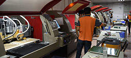
PCBWay is manufacturer specializing in PCB prototyping, low-volume production and PCB Assembly service under one roof. PCBWay strives to be the easiest manufacturer for engineers to work with. PCBWay – PCB Prototype the Easy Way!

Q: 2.Do you accept to assemble the boards that are not made by PCBWay?

Currently we do not use other’s PCB to assemble at our facilities. We offer the PCB fabrication, parts sourcing and PCB assembly in a continuous and smooth manner to save our customer’s time and money.

Q: 3.What files and documents do you request for my PCBA orders?

We need Gerber files, Centroid data and BOM for your PCBA orders. As have already placed your PCB order with us, actually you only need to send the latter two if your PCB Gerber files have included the layers of silkscreen, copper track and solder paste. If your PCB Gerber files are missing any of the above-mentioned three layers, please resend them, as this is the minimum request for PCBA. For the best possible result, please also send assembly drawings, instructions and photos to us to avoid any ambiguous and even mistaken placement of parts, though these are not required by most of the assemblers.

Q: 4.What is Centroid?

Centroid is the special file for assembly used for quickly programming the assembly machines. This is also known as aka Insertion, Pick-N-Place, or XY Data. Some of the CAD tools will automatically generate this file and some not, but you may need to modify the file and then generate the Centroid file. The Centroid file describes the position and orientation of all the surface mount parts, which includes the reference designator, X and Y position, rotation and side of Board (Top or Bottom). Only surface mounting parts are listed in the Centroid.

Q: 5.How do you request for the shipping and marking of the parts for the consigned or kitted order?

We hope you can mark on any individual package or box with the corresponding line number on BOM, manufacturer’s part# or customer’s part#, quantities. A detailed packing list is preferred to enable us to count and check upon receipt of your parts.

Q: 6.What is your requirement on the parts overages for consigned/kitted PCBA?

Unused and excessive parts supplied by you or purchased by us will not be returned by default. If you want the parts to be sent back to you with the assembled boards, please contact your service representitive or make a note on your related order, and let us know which parts to send.

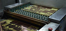
SMT parts which are not supplied on reels should be on one continuous strip of tape.

If you need to assemble the same SMT part in different boards, do not cut them into strips, please keep them in the continuous strip of tape or on the reels.

Resistors, Capacitors, Diodes (0603, 0805, 1206, 2225, SOT, SOD, MELF - packages) require a minimum of 50 pieces and have to exceed the required quantity by 30 pieces. (e.g.: assemble quantity 40 pieces – we will need 70 pieces – this meets our minimum of 50 pieces plus 30 pieces over assemble quantity).

Resistors, Capacitors, Diodes (0201, 0402, miniMelf, miniature packages) require a minimum of 100 pieces have to exceed the required quantity by 50 pieces. (e.g.: assemble quantity 80 pieces – we will need 130 pieces- this meets our minimum of 100 pieces plus 50 pieces over assemble quantity).

A small number of excess(1-5 pieces based on the total quantity of assemblies) is requested for expensive parts such as IC, BGA, QFP, Connectors, etc., this will ensure smooth assembling and shipping your assembled boards on time. If you have any question or doubt, please send more extra or contact us for answers.

Q: 7.Can you source some parts for my assembly?

Yes. This practice is called partial Turn-key. You can supply some parts, and we source the rest of the parts on your behalf. We will ask for your approval for anything that is not sure at our side. In case parts crossing or substitution is needed, we will again ask for your final approval.

Q: 8.Do you assemble BGA? Any special requirement on this?

Yes, We have the ability to handle BGA of 0.25mm pitch with X-ray testing. For BGAs, there are two designs with via on pad and via near pad connected by shorter trace. We need to tent and fill any vias near pad of the BGAs with solder mask to ensure the soldering quality. But for vias on pad, we need to fill via with resin to make sure good soldering quality.

Q: 9. How do you handle the excessive and unused parts?

Excessive parts do exist because we will ask for some percentage of overage for consigned/kitted orders, or we will buy more for the same purpose for those Turn-key orders. You can either ask us to ship back to you these unused parts together with the loaded boards, or keep them in our shelf for your next order. All up to you.

Q: 10.How do you quote the total price of PCBA service?

Our online instant quote system gives the rough idea of the cost of PCBA which include the tooling, laser cut steel stencil, and labor. In case of Turn-key or partial Turn-key PCBA, the cost of parts will be added.

Q: 11.When does the turn-time begin?

Due to the complexity of how to determine the turn time of PCBA services, our policy is that turn-time begins immediately after all the parts and PCBs are ready and all the PCB files (Gerber files/other PCB files, etc.,) , Centroid (Pick & Place PNP file, or XY Data or files in other formats), BOM, and all other necessary data or documents/images/photos are complete for our assembly work.

Q: 12.Is your assembly RoHS Compliant?

Yes. But we also offer leaded PCBA services.

Q: 13.Why do I need to panelize my boards?

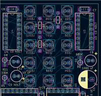
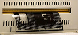
Panelization is needed when your PCB dimension is smaller than 50mmx100mm, or when your PCB is of any shapes (circular, or odd shape) other than rectangle, your boards must be panelized in an array for assembly. As we also fabricate your PCB for you, so once we start fabricating your boards we will have the panelization file (solder paste data), we will transfer the data to PCBA department to create the stencil to match the panelized PCB.

Q: 14.Why do I need to design Break-away Rails (Break-away Tabs) ?

If the clearance between the board’s edge and copper features is less than 3.5mm (138mil), or your boards need to be panelized for some reason, Break-away rails (Break-away tabs) must be added at the two longer paralleled edges of the boards to ensure that the boards can be assembled by the machine. This enables the boards can be processed by the SMT machine.

Q: 15.What if I find any defects or problems after I received your assembled boards?

Defects and problems may occur from time to time, as PCBA is a complex work which involves many details. If you find any defects or problems, please let us know immediately, and we will evaluate and review the problems, and we will make a decision of how to remedy. We will either repair/rework or remake your boards. In case we need the defective boards, we may ask you to send them back to us. We guarantee a functional board in your hand!

Q: 16.What are your PCB Assembly standards?

IPC-A-610 Class 2.

Q: 17.What is your turn time on a Turn-key order?

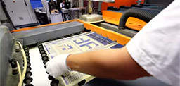
As we need to source all the parts for Turn-key orders, the turn time largely depends on how quick we can get all the parts. We will let you know through everyday email communications. Before all parts are ready, we will fabricate the PCBs and start to make the stencil so that we can start assembly immediately after we get the parts.

Contact Us!

Our customer service
ready for your PCB

+86-571-85317532

quotesI am impressed with the quality of the boards, the delivery time and responce to all my questions. Best price excellent service and speedy delivery. When I need another board I will certainly use this supplier. "

-Bill Robinson Company

quotesспасибо за платы! платы очень хорошего качества. надежный продавец. оперативно отвечал на вопросы. заказ выполнили и отправили очень быстро.Заказываю платы не в первый раз - как всегда только лучшие впечатления. 5+++. 4 числа отправил файлы 26-го забрал на почте в Москве."

-FVL. SKU Company
Front-end data preparation

01.PPE - Pre Production Engineering

Customer supplied data (gerber) is used to produce the manufacturing data for the specific PCB (artworks for imaging processes and drill data for drilling programs). Engineers compare demands/specifications against capabilities to ensure compliance and also determine the process steps and associated checks. No changes are allowed without PCBWay Group permission.

Preparing

02.Preparing the phototools

Artwork Master is PCB production in the key steps, which directly affect the quality of the final product quality,An accurately scaled configuration of electronic data used to produce the artwork master or production master. Artwork Master – The photographic image of the PCB pattern on film used to produce the circuit board, usually on a 1:1 scale.In general, there are three types of Artwork Master:(1) Conductive Pattern  (2) solder mask (3) Silkscreen

print icon

03.Print inner layers

Stage 1 is to transfer the image using an artwork film to the board surface, using photosensitive dry-film and UV light, which will polymerise the dry film exposed by the artwork.
This step of the process is performed in a clean room.
Imaging – The process of transferring electronic data to the photo-plotter, which in turn uses light to transfer a negative image circuitry pattern onto the panel or film.

etch icon

04.Etch inner layers

Stage 2 is to remove the unwanted copper from the panel using etching. Once this copper has been removed, the remaining dry film is then removed leaving behind the copper circuitry that matches the design.
Etching – The chemical, or chemical and electrolytic, removal of unwanted portions of conductive or resistive material.

aoi icon

05.Inner layer Automatic Optical Inspection(AOI)

Inspection of the circuitry against digital “images” to verify that the circuitry matches the design and that it is free from defects. Achieved through scanning of the board and then trained inspectors will verify any anomalies that the scanning process has highlighted. PCBWay Group allows no repair of open circuits.

Lamination icon

06.Lay-up and bond (Lamination)

The inner layers have an oxide layer applied and then “stacked” together with pre-preg providing insulation between layers and copper foil is added to the top and bottom of the stack. The lamination process consists of placing the internal layers under extreme temperature (375 degrees Fahrenheit) and pressure (275 to 400 psi) while laminating with a photosensitive dry resist. The PCB is allowed to cure at a high temperature, the pressure is slowly released and then the material is slowly cooled.

drilling icon

07.Drilling the PCB

We now have to drill the holes that will subsequently create electrical connections within the multilayer PCB. This is a mechanical drilling process that must be optimised so that we can achieve registration to all of the the inner layer connections. The panels can be stacked at this process. The drilling can also be done by a laser drill

copper icon

08.Electroless copper deposition

The first step in the plating process is the chemical deposition of a very thin layer of copper on the hole walls.
PTH provides a very thin deposit of copper that covers the hole wall and the complete panel. A complex chemical process that must be strictly controlled to allow a reliable deposit of copper to be plated even onto the non-metallic hole wall. Whilst not a sufficient amount of copper on its own, we now have electrical continuity between layers and through the holes.Panel plating follows on from PTH to provide a thicker deposit of copper on top of the PTH deposit – typically 5 to 8 um. The combination is used to optimise the amount of copper that is to be plated and etched in order to achieve the track and gap demands.

image icon

09.Image the outer layers

Similar to the inner layer process (image transfer using photosensitive dry film, exposure to UV light and etching), but with one main difference – we will remove the dry film where we want to keep the copper/define circuitry – so we can plate additional copper later in the process.
This step of the process is performed in a clean room.

Plating icon

10.Plating

Second electrolytic plating stage, where the additional plating is deposited in areas without dry film (circuitry). Once the copper has been plated, tin is applied to protect the plated copper.

etch icon

11.Etch outer layer

This is normally a three step process. The first step is to remove the blue dry film. The second step is to etch away the exposed/unwanted copper whilst the tin deposit acts an etch resist protecting the copper we need. The third and final step is to chemically remove the tin deposit leaving the circuitry.

AOI

12.Outer layer AOI

Just like with inner layer AOI the imaged and etched panel is scanned to make sure that the circuitry meets design and that it is free from defects. Again no repair of open circuits are allowed under PCBWay demands.

Soldermask

13.Soldermask

Soldermask ink is applied over the whole PCB surface. Using artworks and UV light we expose certain areas to the UV and those areas not exposed are removed during the chemical development process – typically the areas which are to be used as solderable surfaces. The remaining soldermask is then fully cured making it a resilient finish.
This step of the process is performed in a clean room.

Surface finish

14.Surface finish

Various finishes are then applied to the exposed copper areas. This is to enable protection of the surface and good solderability. The various finishes can include Electroless Nickel Immersion Gold, HASL, Immersion Silver etc. Thicknesses and solderability tests are always carried out.

Profile

15.Profile

This is the process of cutting the manufac-turing panels into specific sizes and shapes based upon the customer design as defined within the gerber data. There are 3 main options available when providing the array or selling panel – scoring, routing or punching. All dimensions are measured against the customer supplied drawing to ensure the panel is dimensionally correct.

Electrical test

16.Electrical test

Used for checking the integrity of the tracks and the through hole interconnections – checking to ensure there are no open circuits or no short circuits on the finished board. There are two test methods, flying probe for smaller volumes and fixture based for volumes.We electrically test every multilayer PCB against the original board data. Using a flying probe tester we check each net to ensure that it is complete (no open circuits) and does not short to any other net.

inspection

17.Final inspection

In the last step of the process a team of sharp-eyed inspectors give each PCB a final careful check-over.Visual checking the PCB against acceptance criteria and using PCBWay “approved” inspectors. Using manual visual inspection and AVI – compares PCB to gerber and has a faster checking speed that human eyes, but still requires human verification. All orders are also subjected to a full inspection including dimensional, solderability, etc.

Packaging

18.Packaging

Boards are wrapped using materials that comply with the PCBWay Packaging demands (ESD etcetera) and then boxed prior to be being shipped using the requested mode of transport.