PCB Prototype the Easy Way
Full feature custom PCB prototype service.
Help Center
Service hotlines
+86 571 8503 9969
9:00 - 18:00, Mon.- Fri. (GMT+8)
9:00 - 12:00, Sat. (GMT+8)
(Except Chinese public holidays)
EN / USD
Welcome to PCBWay
- New Customer?
- Join Free
Home
PCB Instant Quote
CNC | 3D Printing
PCB Assembly
PCB Design
OEM
Product & Capabilities
Why Us?
Feedback
Shared Projects
Module Store
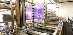
Printed Circuit Boards
- PCB Capabilities

- Advanced PCB
- Advanced PCB Capabilities
- PCB Prototype
- Flex and Rigid-Flex PCBs
- Flexible PCBs
- Rigid-Flex PCBs
- Aluminum PCB
- Metal core PCBs
- High Frequency PCBs
- High-TG PCBs
- Thick-Copper PCBs
- HDI PCB
- LED PCB
- Quick turn PCB Fabrication
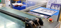
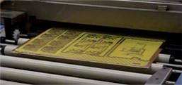
- PCB Prototyping
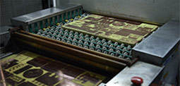
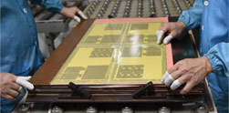
- PCB Production Process
- PCB Products
- PCB Engineering Questions
- FAQ of PCB
SMD-Stencils
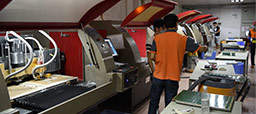
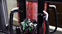
PCB Assembly
- PCB Assembly Overview
- PCB Assembly Capability
- SMT Ordering Necessary Files & Info
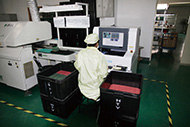
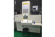
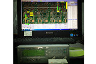
- PCB Assembly Testing Capability
- SMT Assembly Capabilities
- Mixed Assembly Advantages
- Through-Hole Assembly
- BGA Assembly Capabilities
- Components Sourcing
- Panel Requirements for Assembly
- Special Reminders
- File Requirements
- Production Process
- PCB Assembly Products
- PCB Assembly FAQ
PCB Design-Aid & Layout
Drills & Throughplating
Layer buildup
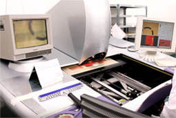
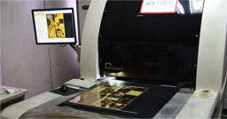
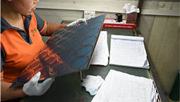
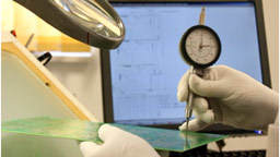
Quality

CNC Machining
Sheet Metal Fabrication
Additional Services