PCB Prototype the Easy Way
Full feature custom PCB prototype service.
Help Center
Service hotlines
+86 571 8503 9969
9:00 - 18:00, Mon.- Fri. (GMT+8)
9:00 - 12:00, Sat. (GMT+8)
(Except Chinese public holidays)
EN / USD
Welcome to PCBWay
- New Customer?
- Join Free
Home
PCB Instant Quote
CNC | 3D Printing
PCB Assembly
PCB Design
OEM
Product & Capabilities
Why Us?
Feedback
Shared Projects
Module Store
Printed Circuit Boards
- PCB Capabilities

- Advanced PCB

- Advanced PCB Capabilities
- PCB Prototype
- Flex and Rigid-Flex PCBs

- Flexible PCBs

- Rigid-Flex PCBs

- Aluminum PCB

- Metal core PCBs
- High Frequency PCBs
- High-TG PCBs
- Thick-Copper PCBs
- HDI PCB

- LED PCB
- Quick turn PCB Fabrication
- PCB Prototyping
- PCB Production Process
- PCB Products
- PCB Engineering Questions

- FAQ of PCB
SMD-Stencils
PCB Assembly
- PCB Assembly Overview
- PCB Assembly Capability

- SMT Ordering Necessary Files & Info
- SMT Assembly Capabilities
- Mixed Assembly Advantages
- Through-Hole Assembly
- BGA Assembly Capabilities
- Components Sourcing
- Panel Requirements for Assembly
- Special Reminders
- File Requirements
- Production Process
- PCB Assembly Products
- PCB Assembly FAQ
PCB Design-Aid & Layout
Drills & Throughplating
Layer buildup
Quality
CNC Machining
Sheet Metal Fabrication
Additional Services



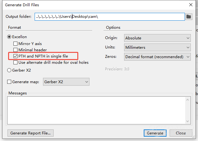
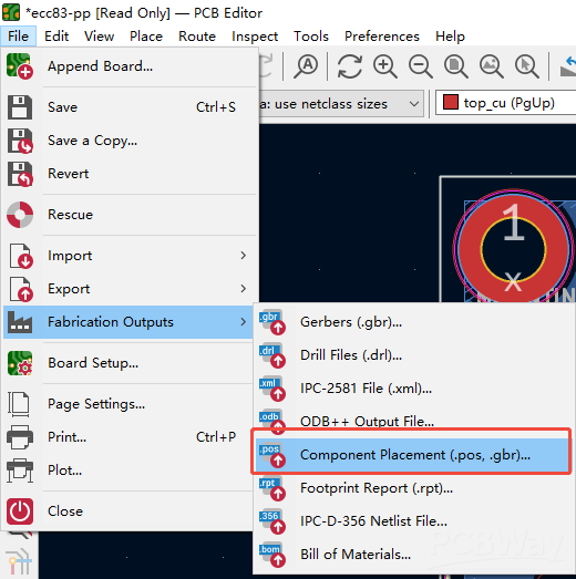
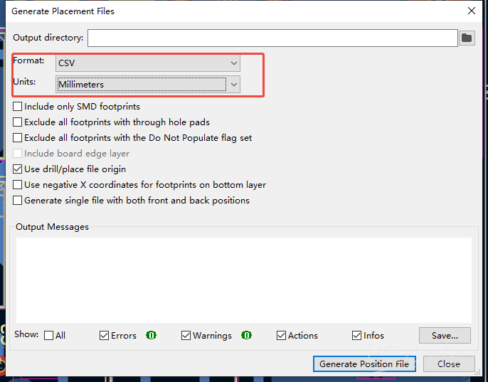
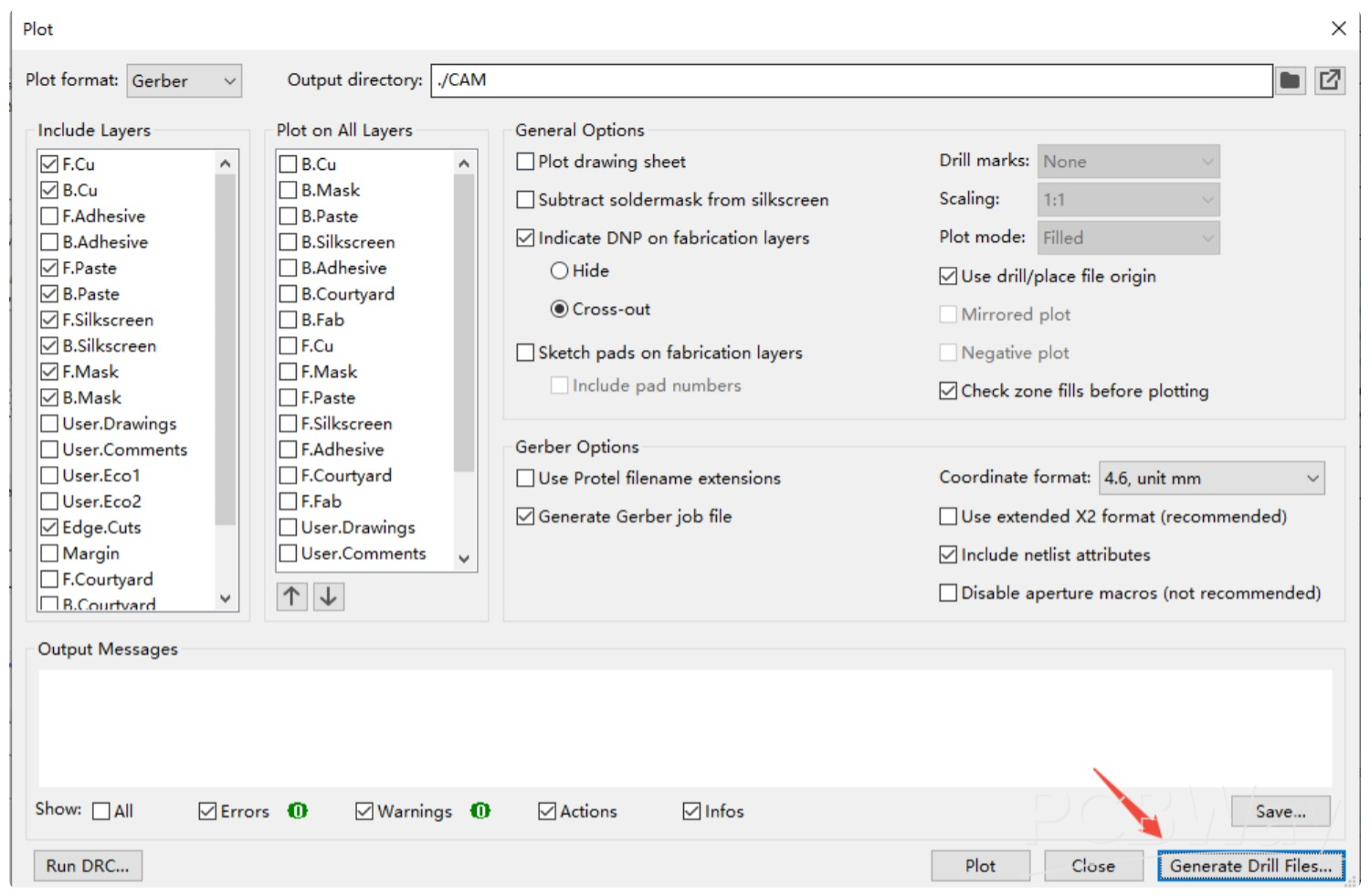 This will open the Drill file settings window, as shown in the image below. Please refer to the image for the settings.