PCB design is the complete process of electronic system development, including schematic design, component selection, PCB layout, rule checking, and manufacturing output. PCB layout, however, is the core execution stage of PCB design, focusing on component placement and routing to transform abstract circuit logic into a manufacturable physical board.
Based on extensive engineering experience, PCBWay PCB design service has summarized a set of practical PCB layout guidelines to help improve performance, reliability, and manufacturability.
PCB layout design is not just placing components and routing traces—it is a system-level optimization process driven by: Signal Integrity (SI); Electromagnetic Compatibility (EMC); Thermal performance; Manufacturability (DFM). The following PCB layout guidelines form the foundation of a reliable design.
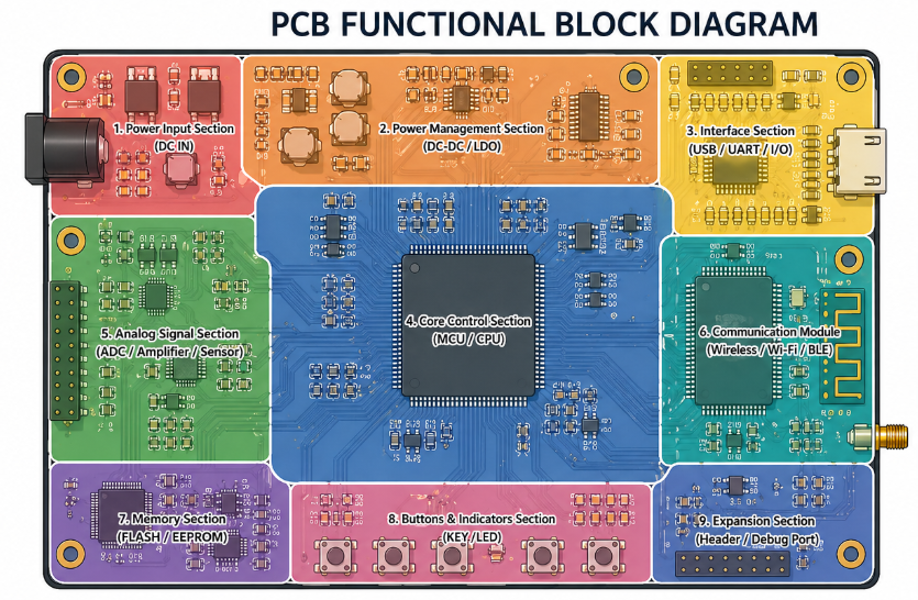
The essence of functional zoning is: group similar functions together and isolate different ones. If zoning is not done properly, EMI issues and signal interference are almost inevitable.
Key PCB layout guidelines:
Especially for complex boards (industrial, automotive) proper zoning directly determines whether EMC testing can pass, making it a fundamental principle in any pcb layout guide.
Not all signals are equal—critical signals must be prioritized.
Critical paths include:
Best practices:
Example: DDR signals must be length-matched before routing general GPIO. Address and control lines belong to critical paths and must be prioritized to ensure equal length and spacing, avoiding crossing with other signals.
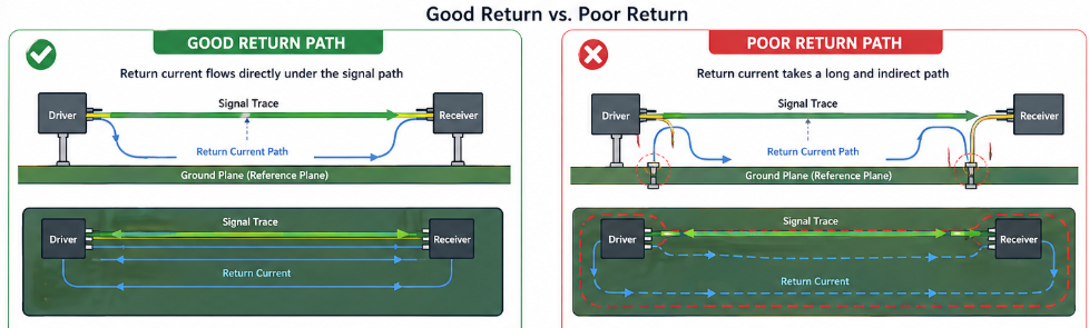
Every signal consists of a signal path and a return path. Ignoring the return path leads to signal distortion, increased crosstalk, and EMI issues.
Core PCB layout guidelines:
The smaller the loop area, the more stable the signal and the lower the interference.
Layout priority is not simply “high-speed first” or “power first”, but based on which factors impact core performance the most. The correct priority is: core power loops > high-speed critical signals > general power > general signals
Reason:
Component placement directly affects signal quality, routing complexity, thermal performance, and production yield.
The purpose of decoupling capacitors is to filter noise and stabilize power supply. However, placement is more important than simply having them.
PCB layout guidelines:
Layering strategy:
Common mistake: placing capacitors far from the IC or stacking them improperly, leading to instability such as reset or malfunction.
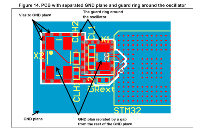
Crystals are the “heart” of high-speed and timing circuits. Poor layout can cause jitter, frequency deviation, or system failure.
Best practices:
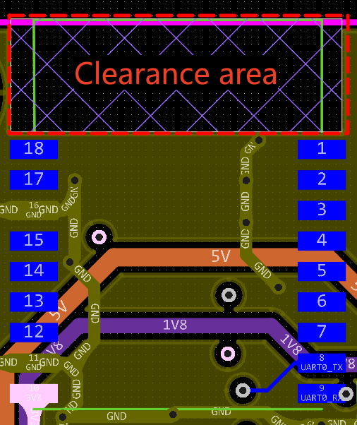
Connectors are the interface between the PCB and external systems, affecting both assembly and EMC.
Core layout guidelines:
The relative position of high-speed components determines routing length, matching difficulty, and interference.
Core principle: place functionally related components close, keep interference sources away
Key points:
EMI and SI are core challenges in PCB layout design. The following pcb layout guidelines help determine when to apply specific techniques.
Not all designs require strict partitioning.
Separation required:
Strict separation is required in these cases.
Separation not required:
Shared ground plane can be used to simplify layout.
Design notes:
Copper planes are the primary heat dissipation medium in a PCB. Proper copper spreading can effectively reduce component temperature.
These structures can cause EMI issues:
For high-power PCBs, thermal design directly impacts reliability and lifespan.
For high-power devices, surface copper alone is not sufficient.
Key parameters:
Related Articles: Thermal Management Design Considerations in PCB Layout
❌️Decoupling capacitors placed too far from IC
❌️Poor crystal routing or grounding
❌️Incorrect zoning
❌️Large power loops
❌️No length matching for high-speed signals
❌️Insufficient thermal design
✅️Decoupling capacitors ≤ 3 mm?
✅️DCDC loop minimized?
✅️Return path continuous?
✅️High-speed signals length matched?
✅️Any floating copper or antenna structures?
✅️Enough thermal vias?
PCB layout may seem like simple component placement and routing, but it is actually a balance of signal integrity, EMC, thermal performance, and manufacturability. Even small mistakes can lead to instability, production issues, or project delays.
If you are facing layout challenges such as EMI issues, unstable signals, or poor thermal design, PCBWay PCB layout design services can help optimize your design, reduce risks, and ensure a stable, production-ready result.


