Smart Insole: Plantar Pressure and Gait Sensing Board
Smart Insole for Athletes — Stage 1 Carrier Board
Efe, Bursa Technical University
A gait lab that fits in a shoe
This project is a smart insole that measures how an athlete's foot meets the ground — pressure under four points of the sole and the motion of the foot — stride by stride, outside the lab.
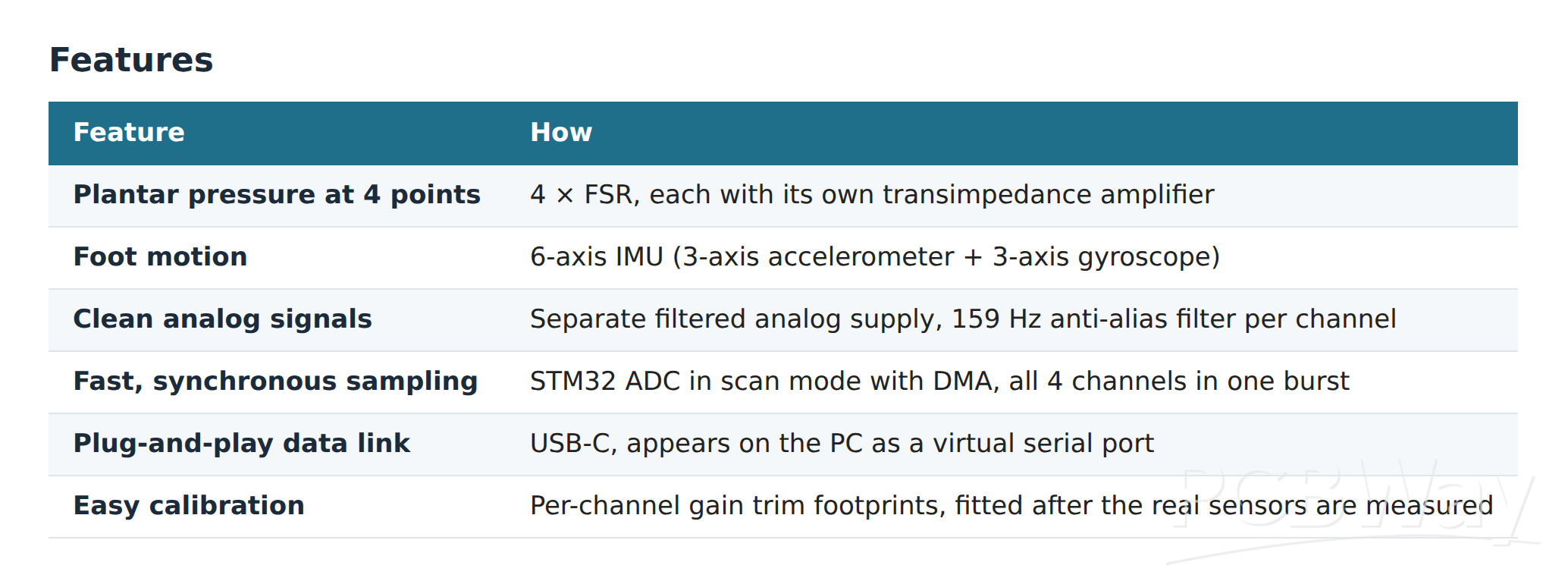
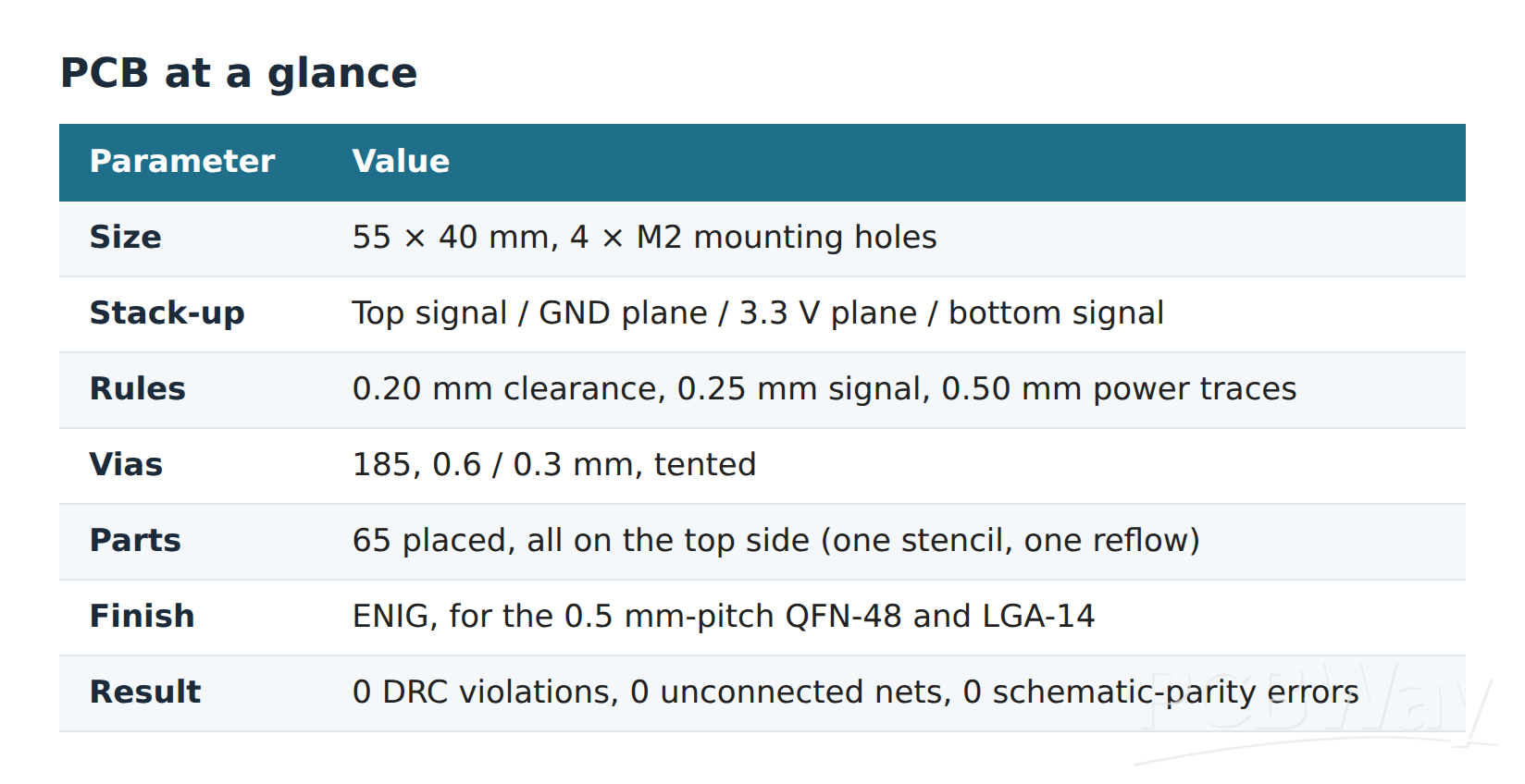
The first hardware stage is a 4-layer, 55 × 40 mm carrier board built around an STM32F411 microcontroller, four force-sensing resistors (FSRs) with their own transimpedance amplifiers, and a 6-axis IMU. The board is fully designed in KiCad, passes DRC with 0 violations, and is ready for fabrication and assembly.
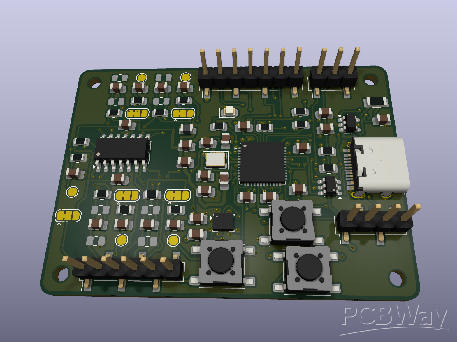
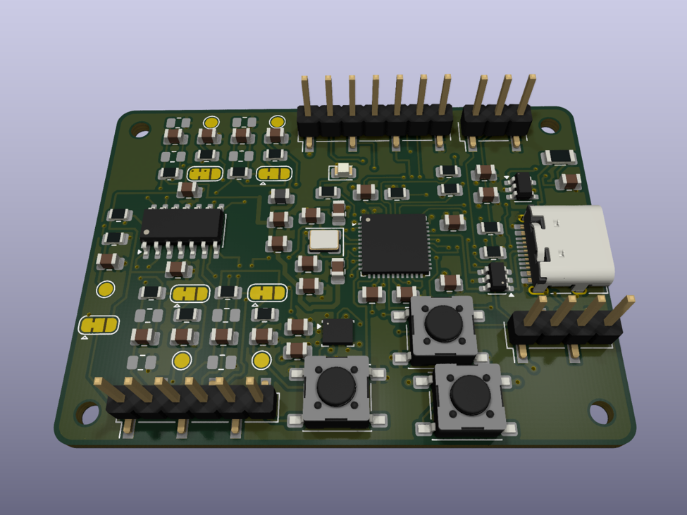
3D render of the Stage 1 carrier board (55 × 40 mm, 4 layers): STM32F411 in the centre, the MCP6004 force-sensor amplifiers on the left, the LSM6DS3TR-C IMU below the MCU, and USB-C on the right.
 The problem
How a foot loads the ground says a lot about an athlete: heel-strike versus forefoot running, left–right imbalance, and changes that come with fatigue or an old injury. Today this is measured with pressure plates, instrumented treadmills or motion-capture systems.
Those tools share three limits:
• They stay in the lab. The athlete runs a few steps on a plate, not a real session on a real track.
• They are expensive. Professional systems are out of reach for students, amateur clubs and most coaches.
• They see a snapshot. A few strides in a test do not show how gait changes over a 10 km run.
A sensor that lives inside the shoe removes all three limits.
The solution
Thin FSRs sit under the insole at four key points of the foot. They connect to a small carrier board worn in a strap at the ankle, which amplifies, filters and digitises the sensor signals, reads a 6-axis IMU, and streams everything to a computer over USB.
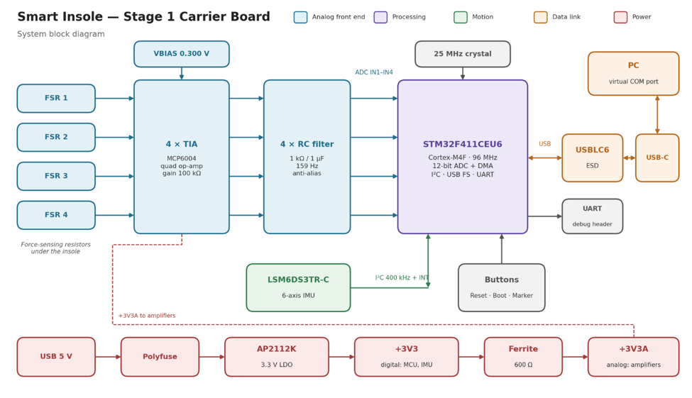
System block diagram: four FSRs feed individual transimpedance amplifiers and anti-alias filters into the STM32's ADC; the IMU connects over I²C, and data leaves over USB-C. A ferrite-isolated analog rail keeps digital noise away from the sensor signals.
 Technical architecture
1. Microcontroller — STM32F411CEU6
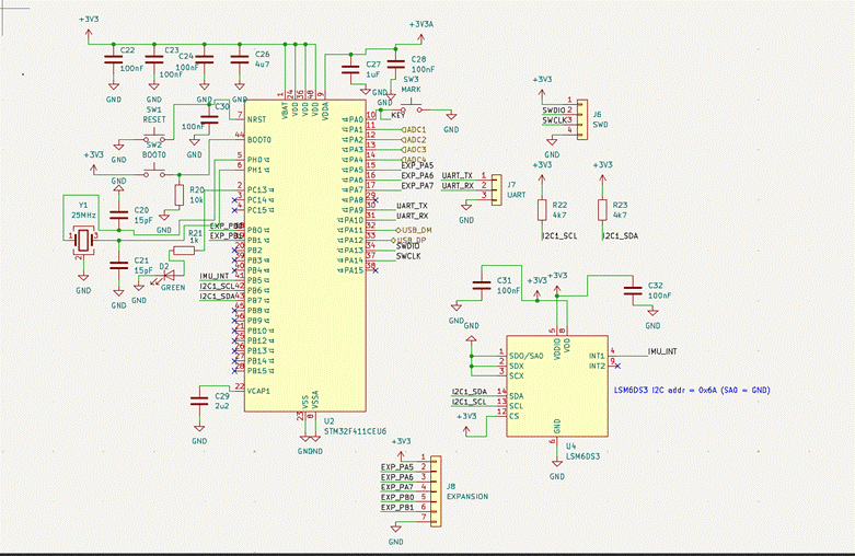
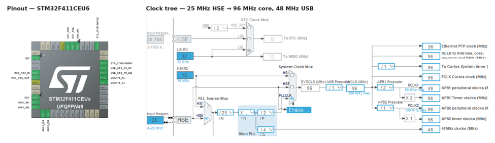
The STM32F411 (Cortex-M4F, QFN-48) runs at 96 MHz from a 25 MHz crystal. The PLL is set so the same clock tree also gives an exact 48 MHz for USB. Its 12-bit ADC samples the four force channels and its USB full-speed peripheral sends data to the PC.
The crystal load capacitors were calculated, not copied: C = 2 × (CL − C_stray) = 2 × (12 pF − 4 pF) = 16 pF, so 15 pF C0G parts are used. Reset, BOOT0 and a user "marker" button are on board; the marker lets the athlete tag a moment in the recording.
Main schematic sheet: STM32F411CEU6 with its 25 MHz crystal, decoupling, reset/boot/marker buttons and SWD/UART headers, plus the LSM6DS3TR-C IMU on I²C (address 0x6A).
 2. Force-sensor front end — 4 × transimpedance amplifier
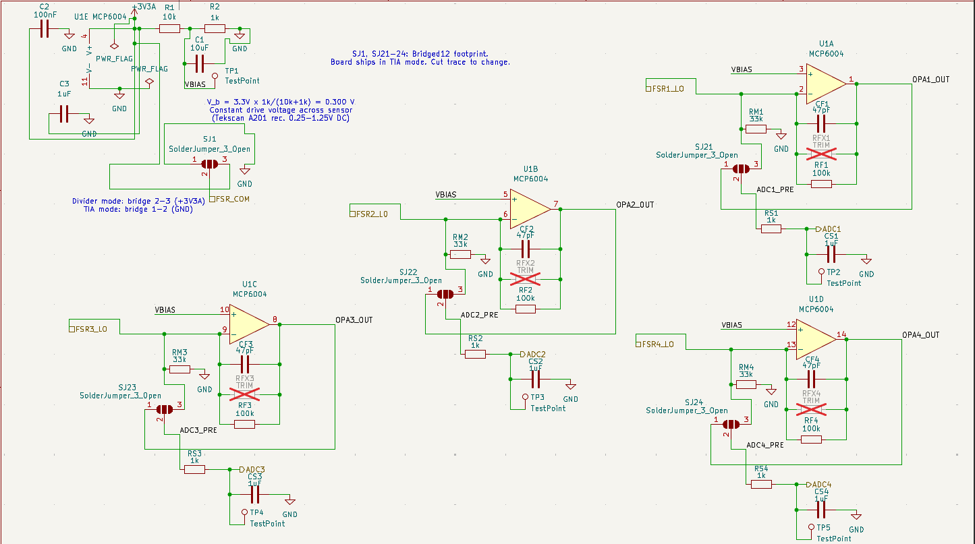
An FSR's resistance drops as force rises. Instead of a simple voltage divider, each sensor drives its own transimpedance amplifier (one channel of an MCP6004 quad op-amp), which gives a more linear response to force. All four stages are biased from a shared 0.300 V reference routed as a star to the op-amp inputs.
Output of each channel:
V_out = 0.300 V + (0.300 V / R_FSR + 0.300 V / 33 kΩ) × 100 kΩ
The output reaches the 3.3 V rail when the sensor falls to about 14 kΩ. Each channel then passes an RC low-pass filter (1 kΩ / 1 µF, 159 Hz) before the ADC. FSRs vary about ±25 % part to part, so each channel has an unpopulated trim resistor footprint in parallel with the 100 kΩ feedback resistor, fitted after the real sensors are measured.
Force-sensor front end: four transimpedance amplifiers (MCP6004) biased at 0.300 V, each followed by a 159 Hz RC anti-alias filter. RFX1–RFX4 are gain-trim positions, fitted after the real sensors are measured.
 3. Motion — LSM6DS3TR-C 6-axis IMU
The IMU gives 3-axis acceleration and 3-axis rotation over I²C (400 kHz, address 0x6A). Its interrupt line goes to the MCU, so the firmware reads new samples as soon as they are ready. The original LSM6DS3 is obsolete, so the board uses the pin-compatible LSM6DS3TR-C, with the LSM6DSO as a second-source option.
4. Power and USB
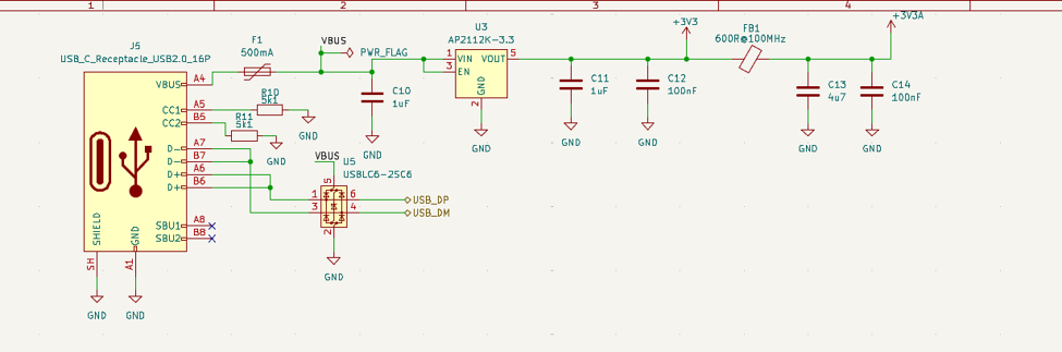
The board is powered from USB-C through a polyfuse and an AP2112K 3.3 V LDO. The analog amplifiers get their own rail (+3V3A) behind a 600 Ω ferrite with separate decoupling, so digital switching noise stays out of the sensor signals. A USBLC6 protects the USB data lines from ESD.
Power and USB: USB-C input through a polyfuse into an AP2112K 3.3 V LDO. The analog rail (+3V3A) is split off behind a 600 Ω ferrite with its own decoupling, and a USBLC6 protects the USB data lines from ESD.
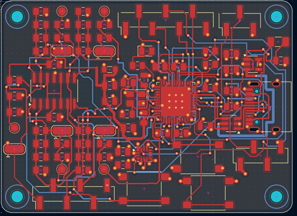
 A few decisions that shaped the layout:
• Power by planes. Every supply pin reaches its plane through a short stub and via, so power currents never share a path with the analog signals.
• Analog rail as a trace tree, not a third plane. Two overlapping planes would form a capacitor that bypasses the ferrite at high frequency.
• Crystal rotated 180°. Both oscillator traces now run on the top layer with no vias (6.4 mm and 9.4 mm), with a ground guard between them.
• No hand soldering needed. Configuration jumpers ship bridged in copper and can be cut later to reconfigure.
PCB layout in KiCad, top (red) and bottom (blue) copper. The two inner layers are solid GND and +3.3 V planes. 185 vias, 0 DRC errors.
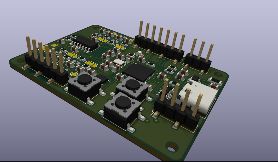
 3D view of the assembled board: all 65 parts on the top side for single-pass reflow, USB-C on the right edge, headers for the sensor cable, SWD and UART.
 Firmware — already in progress
While the board is in review, I started the firmware in STM32CubeIDE so it is ready the day the boards arrive. It is being developed on an STM32F411 development board with the same chip, then moved to this board.
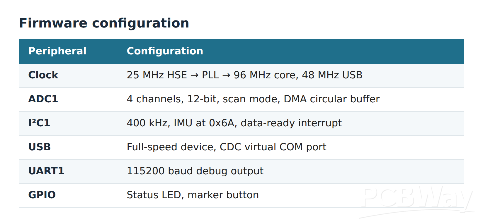 Next firmware steps: stream the four force channels and IMU data over USB, then build a simple PC viewer to plot them live.
STM32CubeMX configuration: ADC1 on PA1–PA4, I²C1 on PB6/PB7 with the IMU interrupt on PB5, USB on PA11/PA12, UART1 on PA9/PA10. The 25 MHz crystal drives the PLL to 96 MHz for the core and exactly 48 MHz for USB.
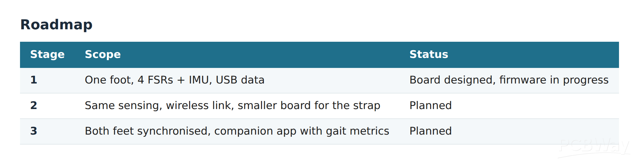 Stage 1 exists to prove the analog front end and collect real calibration data before the design is shrunk and made wireless.
Why PCBWay
This board is not something I can build by hand: a 0.5 mm-pitch QFN-48, an LGA-14 IMU with 0.15 mm pad spacing, a 4-layer stack-up and an ENIG finish all need professional fabrication and machine assembly. The order I am asking support for is 5 PCBs, with 3 of them assembled.
With these boards I will measure the four sensors, fit the calibration resistors and record the first real running data. I will share the test results, photos and lessons learned on this project page, and credit PCBWay in every write-up and presentation of the project.
About me
I am Efe, a third-year Electrical and Electronics Engineering student at Bursa Technical University, Turkey. I designed this board end to end on my own — concept, schematic, component selection, placement, routing and manufacturing files — and I am now writing its firmware. I want to build a career in hardware design, and this project is my first complete step from an idea to a manufacturable product.
Apply for sponsorship >>- Comments(0)
- Likes(0)