Raiden S0-1
This one started while I was waiting. I'm building a fixed-wing UAV for SUAS 2026, where the telemetry link runs on an ESP32 over DroneBridge and the ground station is my own software. Competitions move in long pauses, and rather than sit through one I decided to widen the electronics side instead of just the flying side. Going from using someone else's ESP32 board to drawing my own was the obvious next step.
So I wanted a development board built around a bare ESP32-S3FN8 in a QFN-56 package rather than a pre-made module,because that is where the actual work is. The 0.4 mm pitch fanout, the crystal network, the USB-C front end, the RF matching network and the 50 Ohm antenna feed are all mine to get right. A board built on a module hides every one of those from you.
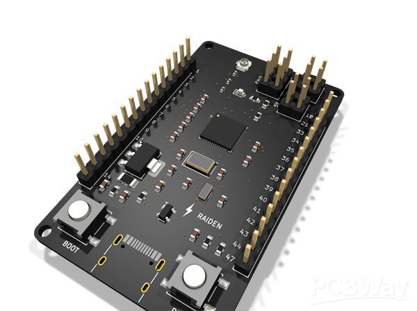
The board is 36 x 60 mm on four layers, with a solid ground plane on In1 and a 3.3 V plane on In2. USB-C goes straight to the chip's native USB, so there is no USB-to-UART bridge anywhere in the path. Power is an AZ1117C-3.3 with a PTC on VBUS and ESD protection on the data lines. Around 30 GPIO come out on two 1x15 headers, and separate 5 V, 3.3 V and GND rails run along the board edge so a sensor can be fed without a breadboard at all. RF is a u.FL antenna with a pi matching network and a keepout under the connector.
Everything is published under CERN-OHL-P v2: the KiCad 9 schematic and PCB, the complete fabrication package (11 Gerber layers, Excellon drill, drill map, pick-and-place, schematic PDF, BOM with manufacturer part numbers), renders, and a build journal covering roughly 60 hours of design work across six sessions, mistakes included.
Two of those mistakes are why I trust the current revision. Ten traces looked perfectly connected and were short by 60 microns, and only a netlist check found them. Later, a reviewer glancing at a render noticed the USB-C connector sat 3.75 mm inside the board edge, so a cable's overmould would have hit the PCB before the plug ever seated. Every automated check I owned had passed on a board that could not have been plugged in. Both are fixed, and I verify with kicad-cli now instead of by eye.
Current state: ERC 0 errors, DRC 0 errors, 0 unconnected nets, 0 schematic-parity issues. The remaining DRC warnings are five deliberate library mismatches, mostly the intentional RF keepout and the minimal mounting-hole footprint.
Raiden S0-1 Images
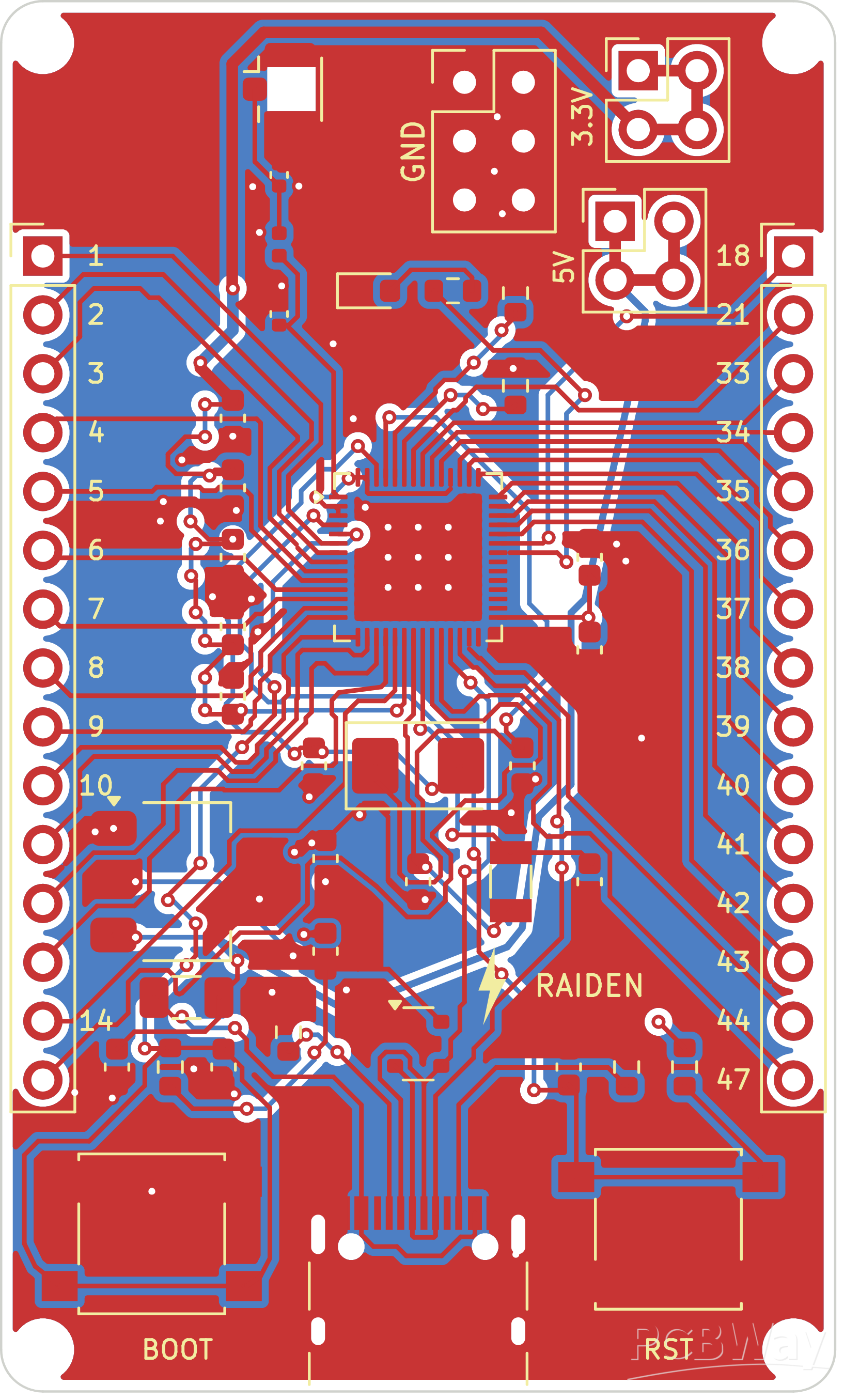
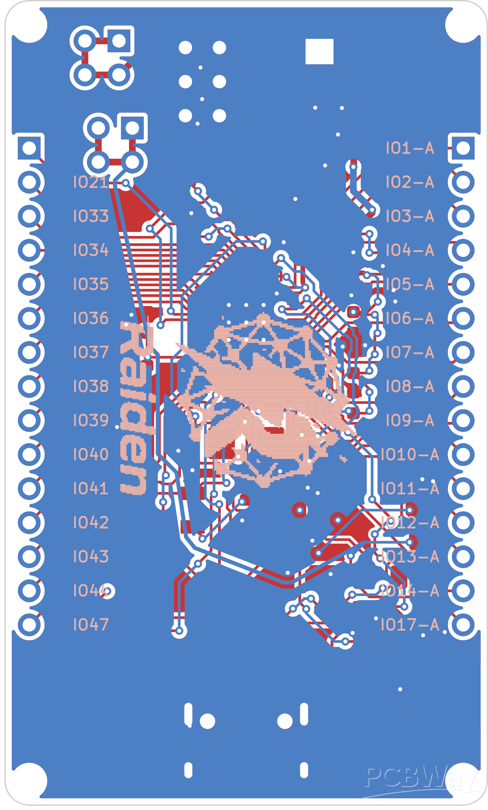
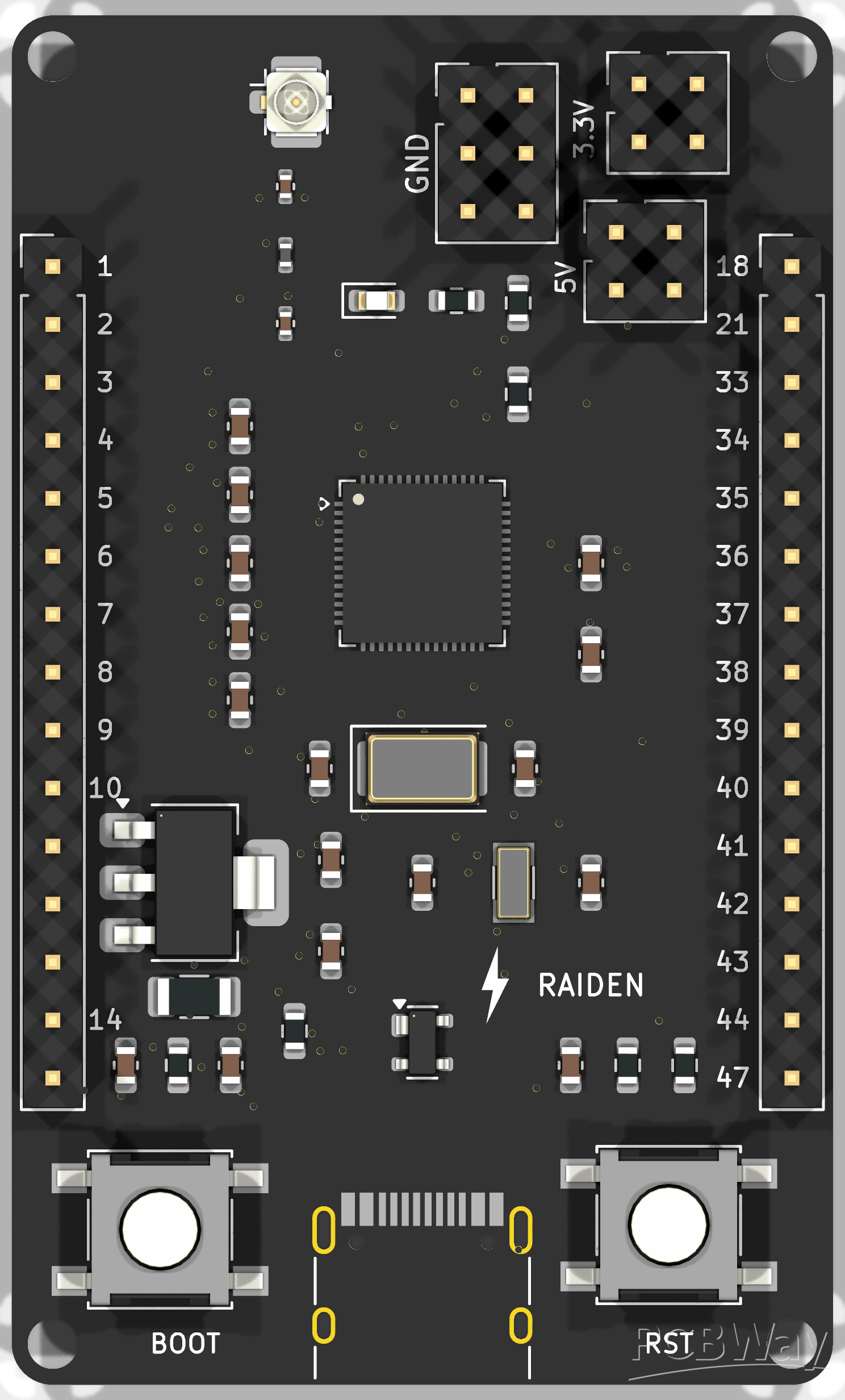
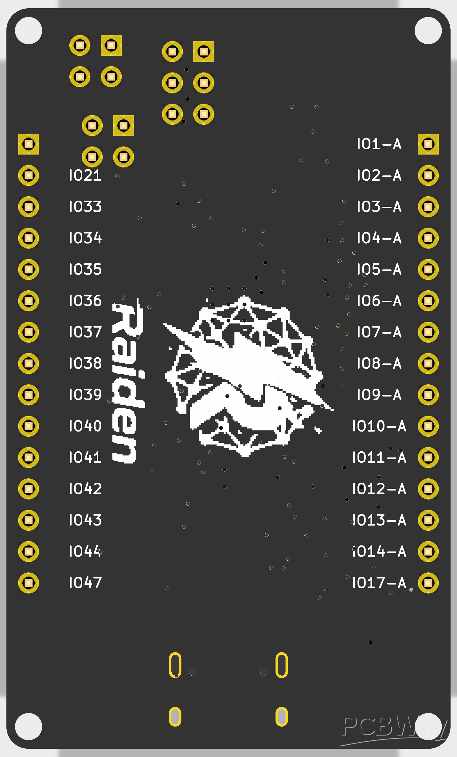
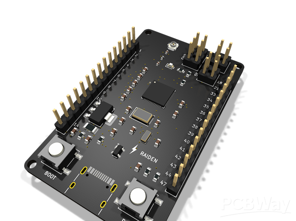
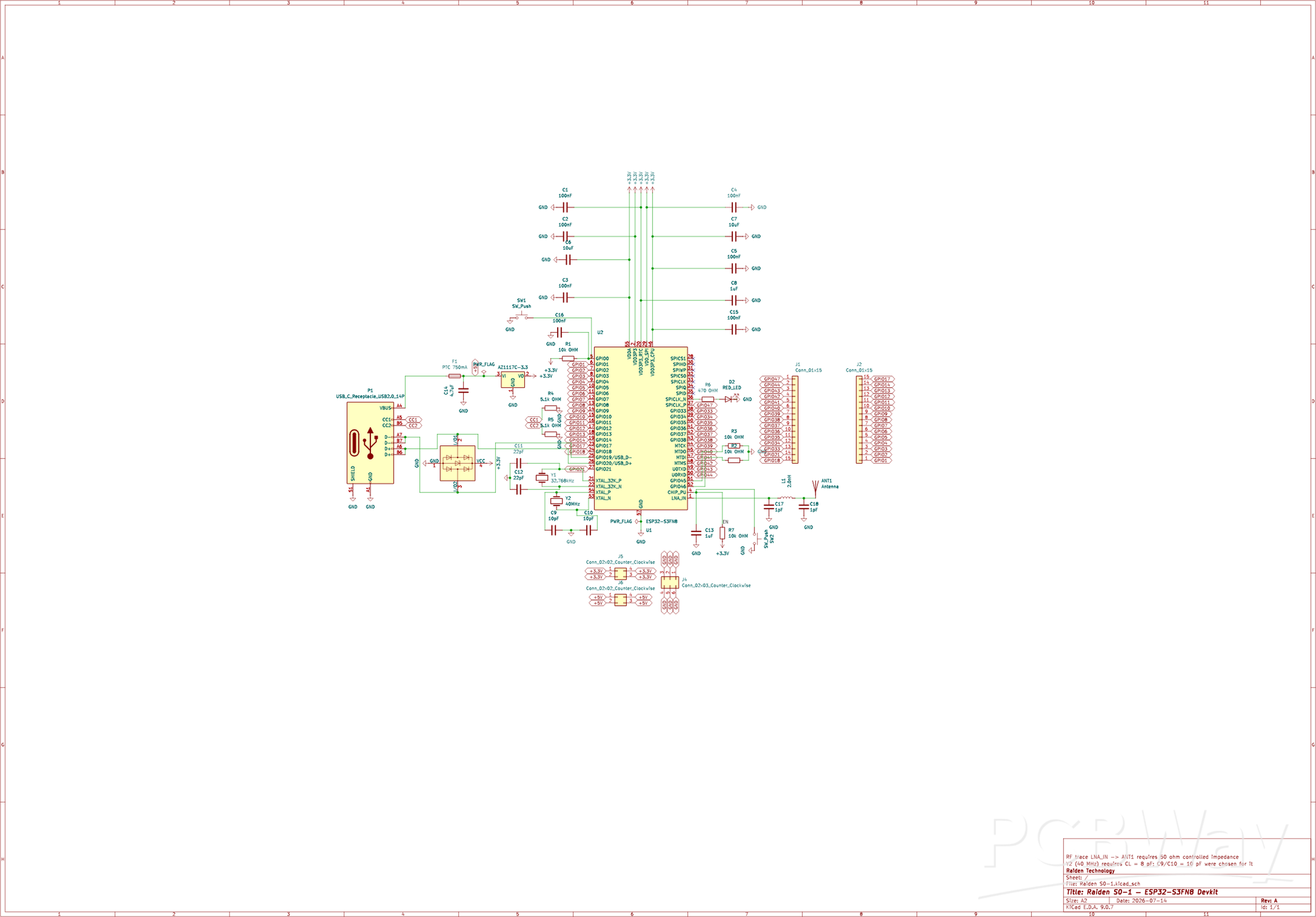
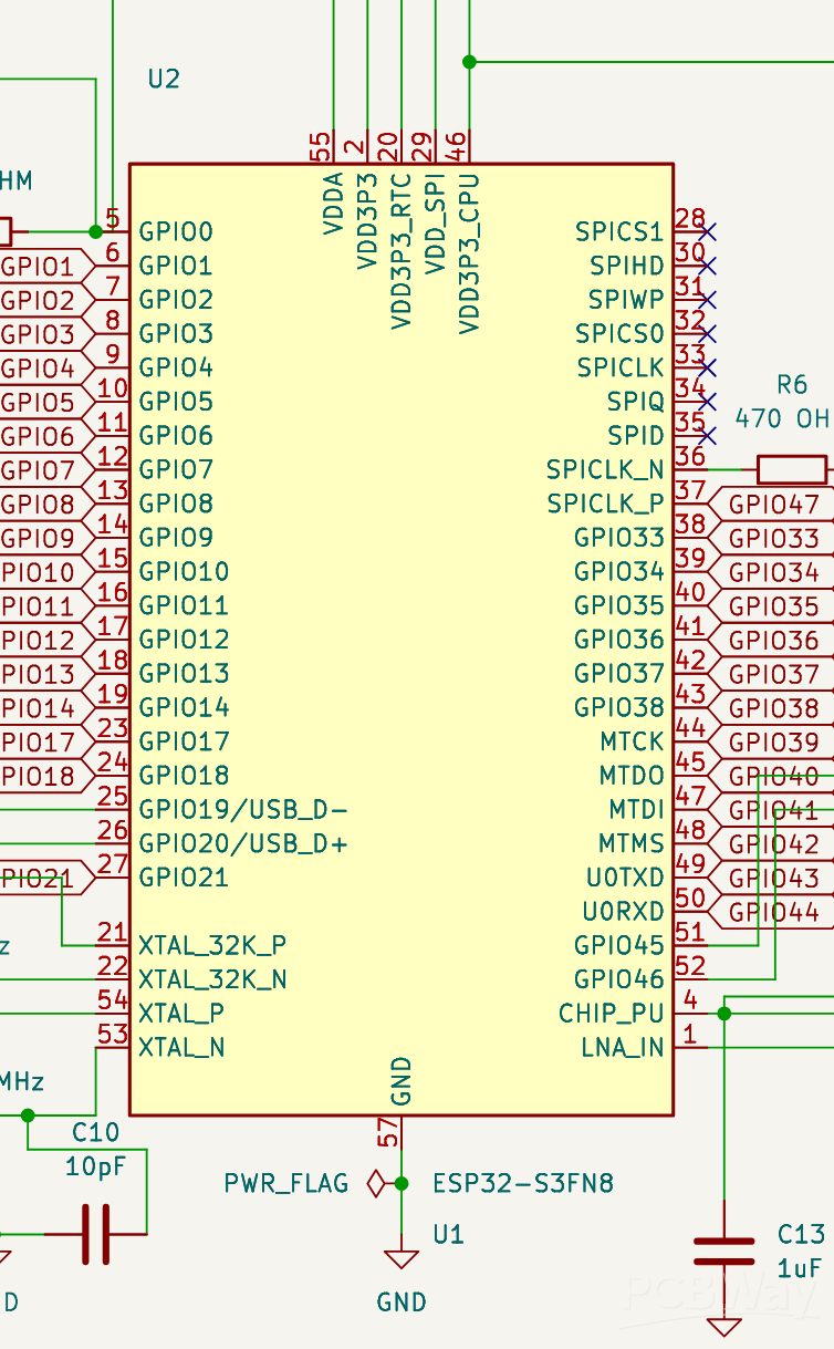
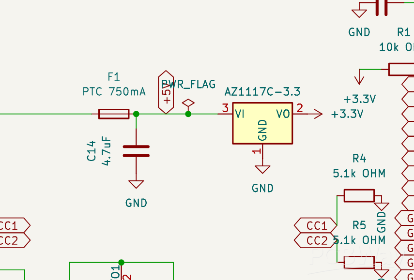
The part in the middle is an ESP32-S3FN8, a QFN-56 package, 7 mm square with 0.4 mm pin pitch. Two cores at 240 MHz, Wi-Fi, Bluetooth LE 5, and 8 MB of flash built into the package instead of sitting next to it as a second chip.
Almost every ESP32 board on the market starts from a pre-certified module dropped onto a breakout. The crystal, the decoupling, the RF matching and the antenna all live sealed inside that module, so the board around it comes down to headers and a regulator. I did not want to build that board. I wanted to build the thing the module hides. So here the crystals, the power path, the decoupling and the RF front end are all mine, worked out from the chip datasheet and the hardware design guidelines instead of copied from someone else's reference layout. That one decision is why this took as long as it did, and it is also why there is anything here worth reviewing.
Power
USB-C brings 5 V in on VBUS. The first thing it hits is a 750 mA resettable PTC fuse, so a short further down the board trips the fuse and not the host port. After the fuse, the 5 V rail feeds a 4.7 µF bulk capacitor and then an AZ1117C-3.3 in SOT-223. That regulator makes the 3.3 V rail everything else runs on.
I picked the C variant of the 1117 on purpose: it is the ceramic-stable one. A regulator that needs a tantalum or an electrolytic on its output to stay inside its stability region is a trap on a board where every other capacitor is a 0603 ceramic.
The regulator's thermal tab is not floating. It ties to the 3.3 V net, drops to the plane through a via in the pad, and sits in a local 3.3 V pour. The 1117 is a linear part, so the gap between 5 V in and 3.3 V out leaves as heat through that tab. It has real work to do once Wi-Fi is transmitting and somebody has hung a load off the rail headers. My own budget for external draw on the 3.3 V rail is about 200 mA, for exactly that reason.
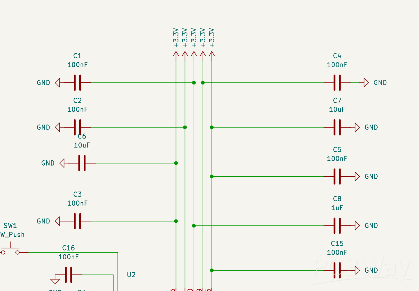
Decoupling comes to seven 100 nF capacitors, two 10 µF, one 1 µF and one 4.7 µF, spread over the chip's supply pins. The 5 V that comes back out on its own header is tapped after the fuse, not from raw VBUS.
USB
The USB-C connector goes straight into the chip's own USB peripheral. No CH340, no CP2102, no USB-to-UART bridge anywhere on the board. The ESP32-S3 has USB in silicon. Adding a bridge would mean paying for a part, a second clock domain and a driver install, all to reach a peripheral that is already there.
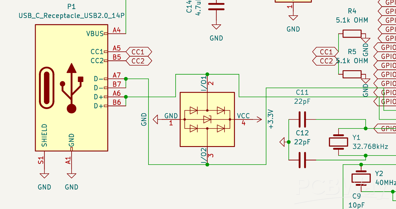
Both CC lines on the fourteen-pin receptacle get their own 5.1 kΩ pulldown. That is what tells a Type-C source to actually hand over 5 V instead of sitting there doing nothing. The two halves of the connector are bridged, so the cable works either way up.
A PRTR5V0U2X ESD array sits across the data lines, shunted between D+ and D− with its supply pin on 3.3 V. A static hit into the connector then has somewhere to go that is not the chip's USB pins. UART0 still comes out on the headers for the times when native USB is not what you want.
Clocks
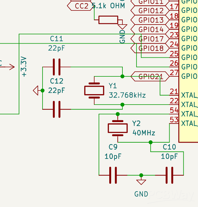
Two crystals. The main one runs at 40 MHz and is specified for an 8 pF load, which is matched by 10 pF load capacitors on the board.
Those numbers have to agree. The crystal sees the two load capacitors in series, plus the stray capacitance of the traces and the pins. Buy a crystal cut for a different load and the oscillator either runs off frequency or refuses to start at all. I wrote CL = 8 pF on the schematic canvas, again in the bill of materials as part of the manufacturer part number, and a third time in the fabrication notes. It is the kind of detail that falls straight through the gap between a repository and a parts order.
The second crystal is a 32.768 kHz part with 22 pF load capacitors, feeding the real time clock domain. That lets the chip keep time through deep sleep without the main oscillator running.
RF front end
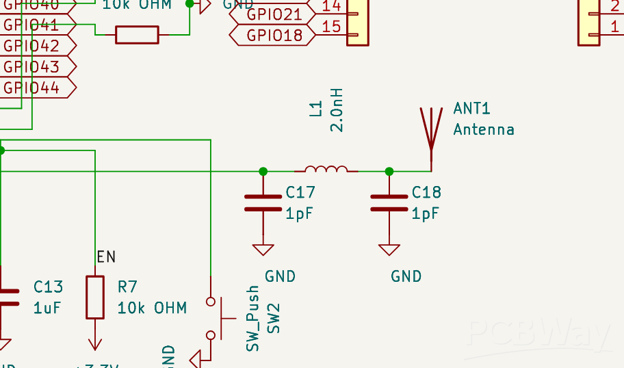
There is no antenna on the board. There is a U.FL connector, fed through a pi matching network of 1 pF, 2.0 nH and 1 pF, so the board takes an external antenna on a pigtail. No printed trace antenna.
That was a trade I made on purpose, not a shortcut. A printed antenna costs nothing in parts, but it only behaves the way its simulation promises when the ground pour, the keepout and the surrounding enclosure all match the reference design, and I have no way to measure whether mine do. A connector costs a part and hands the problem to an antenna somebody else has already characterised.
The copper pours are cut back under and around the connector, with a deliberate keepout on every layer, so the ground plane does not sit right under the launch. The feed trace is drawn at 0.2 mm, with 50 Ω single ended as the intent. That word "intent" is doing work there, and I come back to it in the honest section below.
What comes out to the pins?
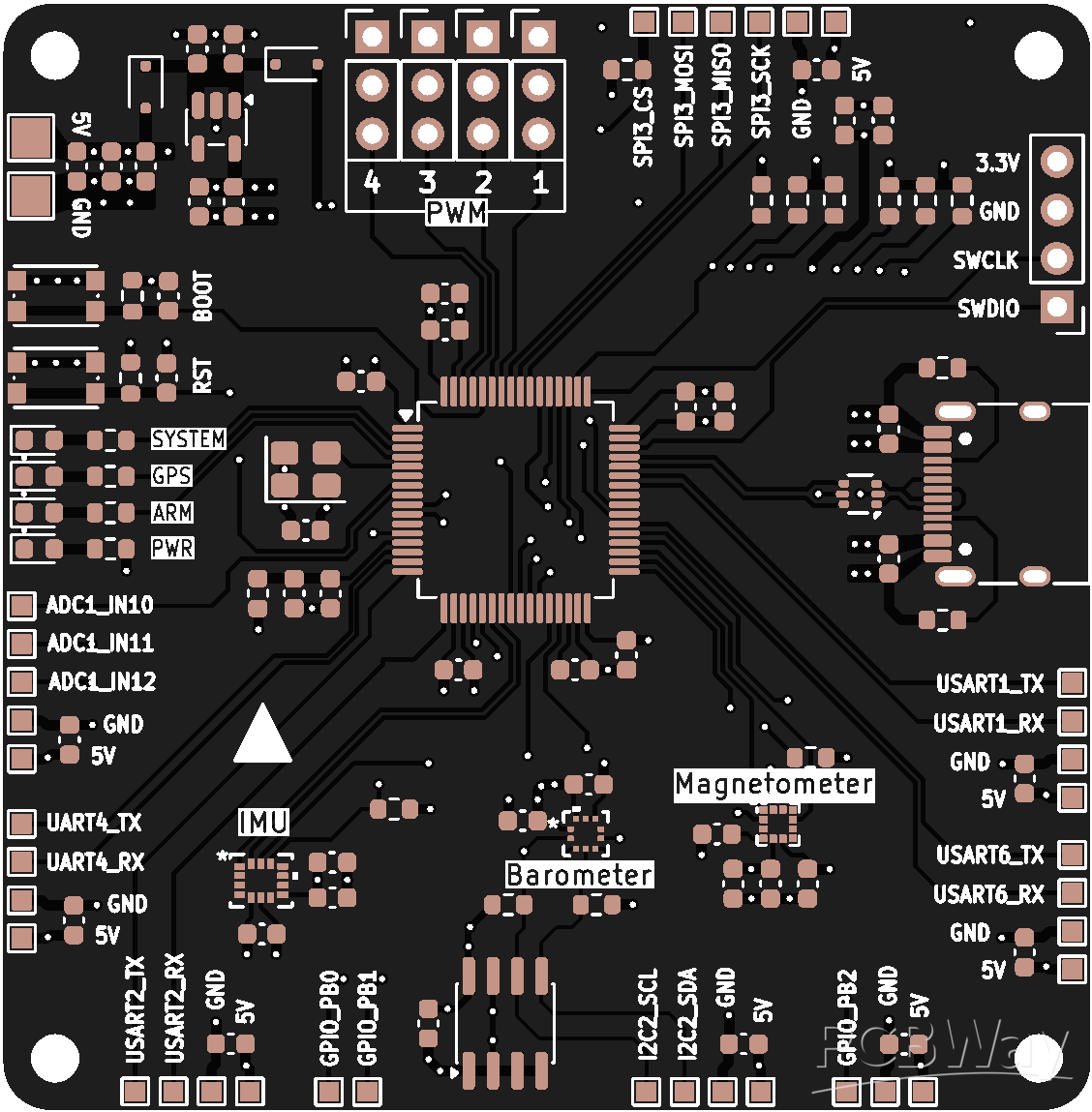
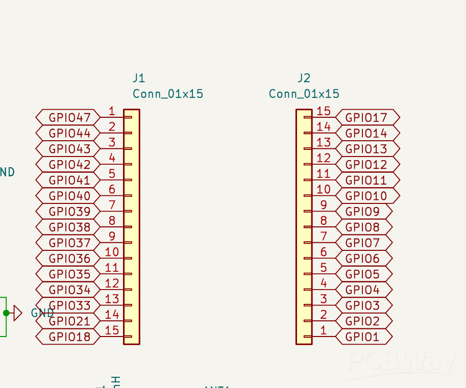
Thirty GPIO leave on two fifteen-pin headers at 2.54 mm, one down each side. There is not enough room to print both labels on the same face, so the front silkscreen carries the position number of each pin and the back carries the actual IO name.
Along the board edge there are separate rail headers: six ground pins, four 3.3 V and four 5 V. A couple of sensors can be powered straight off the board with no breadboard rail in between. That is the thing I waste the most time wiring around when I prototype.
BOOT and RESET are debounced in hardware, not left to firmware. There is a user LED on GPIO48 behind a 470 Ω resistor, and four M2 mounting holes, one per corner. The finished board is 36 by 60 mm, black soldermask, white silkscreen, 42 placements drawn from 24 lines of bill of materials.
Stackup and layout
Four layers: signal on top, a solid ground plane, a solid 3.3 V plane, signal on the bottom.
It did not start there. Version one was two layers, and it routed almost all the way before it stopped dead. What was left were the power and ground connections around the QFN, and there was nowhere for them to go with both outer layers already full of signal. I tried a 3.3 V pour on the top layer and got zero polygons filled. Hard to argue with that: the region was not awkward, it was full.
Going to four layers did not buy routing space, and this is the part I would want someone to take away from it. Both inner layers are solid planes with no traces on them at all, so the signal layer count is still two. What the extra copper bought was a destination. Every power and ground pin now drops straight into its own plane through one via, instead of hunting for a path across the board. That is why most of the 114 vias here are stitching, not routing. One more thing worth knowing before your first four-layer board: the inner layer numbering is not what you would guess, and the stackup has to be set in the GUI. Do not assume it from the file.
How I check it?
I do not trust my eyes on this board. Nothing here is verified by looking at the screen. Every check runs against the file itself with kicad-cli, so I can re-run the whole thing after any change and compare it against the previous result instead of trying to remember what used to be true.
Right now ERC reports zero errors. DRC reports zero errors and zero unconnected items.
Six DRC warnings are left in on purpose. All six are local footprint edits I made deliberately: the RF keepout under the U.FL connector, and the four M2 holes. Three schematic parity notices stay for the same reason. The two shell pads of the U.FL connector and the thermal tab of the regulator carry copper on the board but have no matching pin in their symbols. I list all nine out loud, because a board that reports a perfectly clean sweep with no explanation attached usually means someone turned a rule off.
Two things bit me hard enough to be worth passing on. First, the connectivity report can be confidently wrong about location. A zone reporting a missing connection kept pointing at its own anchor coordinate instead of the actual gap. Finding the real isolated copper pockets took a union-find pass over every track, via and pad, using proper shape collision instead of centre points. Second, a hand-drawn trace can stop sixty to a hundred microns short of a pad and still look completely connected on screen. Ten of mine did. Invisible to the eye, obvious to the file.
The routing review
In August someone in the Hack Club hardware channel looked at this board and said the routing was messy, that there were too many sharp angles, and that a signal trace carrying more than two or three vias is asking for trouble, because via inductance is what turns a clean edge into a glitch. Fair. So I went through it properly instead of tidying the parts that were easy to see.
I wrote a script that walks every track joint, measures the direction change, and reports anything turning more than 45 degrees. It found 35.
Fifteen were real corners out in open copper. All fifteen are gone. Some I chamfered, some I deleted outright, because they turned out to be spikes where a trace ran out and came straight back. Two were jogs about fifty microns long, shorter than the trace width itself, left over from earlier edits.
The other twenty turn inside a pad. That is normally fine, because pad copper is wider than the trace and the sharp wedge never actually forms. I did not want to take that on faith. Two traces leaving a point with a separation angle s keep their edges touching for a length of w divided by twice the sine of half that angle. If that length is shorter than the distance to the pad edge, the wedge closes inside the pad and never reaches open copper. Eighteen passed with room to spare. Two did not, both on narrow QFN power pins, where the wedge poked about forty microns past the pad edge. Those two got chamfered too.
On via count, both USB data lines came down from four each to two, and the crystal's negative line from four to two. One of those only became possible after I spotted a 9.4 mm 3.3 V rail running across the back that the USB lines were diving under in order to cross. The board already carries a whole 3.3 V plane, so that rail did not need to exist. One via down to the plane, one deleted trace, and the channel opened up.
Then I asked a blunter question: which vias are load bearing at all? I answered it by pulling each one in turn and asking the connectivity engine whether the net still held together. That is how I found the crystal's positive line running two parallel routes side by side, from its load capacitor to the crystal, with four vias between them where two would do. Left over from an earlier session, never noticed by anyone, me included. On a 40 MHz clock a redundant parallel path is not free, so the longer route is gone. The same check turned up a duplicate stub on the antenna feed, sitting inside a longer trace that already covered it.
Every signal via on the board is now load bearing: pull any one of them and something disconnects. The only vias that can come out harmlessly are ground and 3.3 V stitching, which is what stitching is for. The total went from 121 to 114.
One thing I refused to do. The same connectivity check flagged roughly 20 mm of trace across 25 nets as removable. Most of that was the last section of a trace where it enters a pad, flagged only because it overlaps the pad copper. Cutting those would end traces at pad edges, which is the exact failure that had already bitten me once. Same reasoning for the short traces around the decoupling capacitors: redundant for DC is not redundant for decoupling, and DRC cannot tell me the difference.
Every step went back through DRC afterwards. The board finished where it started. Zero errors, zero unconnected items, the same six deliberate warnings.
What I know is still wrong?
I would rather write this section myself than have a reviewer find it for me.
The RF trace is not impedance verified. It is drawn at 0.2 mm with 50 Ω single ended as the intent, but I never defined a controlled impedance stackup, so that 50 Ω is an assumption and not a calculated or measured number. The matching network values are starting points. There is no vector network analyser behind them.
Three nets still carry more than three vias: GPIO0 with eight, the crystal's positive line with four, the enable line with four. None of them are spare copper any more, since I checked each one individually. Every one is a genuine crossing over another net. Removing them means ripping up and rerouting the neighbours as well, and that is manual work I have not done yet.
The crystal is also on the wrong side of the chip. Its pins come out of the top edge of the QFN and I placed the crystal below, so those traces run all the way around. That is a placement mistake, not a routing one, and fixing it properly means moving parts in the next revision.
The honest headline: this board has never been manufactured. The design is finished, the fabrication files are generated, and none of it has been proven on real copper.
What is published?
Everything is public under CERN-OHL-P v2 at github.com/RaidenTechnology/raiden-s01
The repository holds the KiCad 9 schematic and PCB, the full fabrication package with eleven Gerber layers, the Excellon drill file, the drill map, the pick and place CSV, the JLCPCB bill of materials and component placement list, and the schematic PDF. There is also a bill of materials with manufacturer part numbers down to every passive, the rendered images, and JOURNAL.md.
JOURNAL.md is a written log of roughly sixty hours of design work across six sessions, mistakes included, in the order I made them and with what each one cost. It says openly that it was compiled after the fact and not committed as I went, because I would rather publish an honest reconstruction than a faked commit history.
The licence is permissive on purpose. Anyone can take this board, change it, build it and sell it without asking me first.
Why didn't I produce?
After finishing the circuit board, I wanted to manufacture it, and I would have if I could have found a good price. However, there were parts that couldn't be soldered by hand, so I did some research to see if there were any companies that offered assembly services. There were, but the price was around $110, and they would send some parts unassembled. Even with a discount coupon, it only went down to $100. I just wanted to manufacture it, but if I did, I would have to give up my AI subscription, which helps in many areas. So I had to choose between the two, and I chose the subscription for software and other tasks. I didn't manufacture the board. I still want to manufacture it now, but I need to find both a good opportunity and a good price. I hope this has been helpful for you.
Apply for sponsorship >>- Comments(0)
- Likes(1)