RFI-PaCe (Team Australia) - PocketQube satellite payload
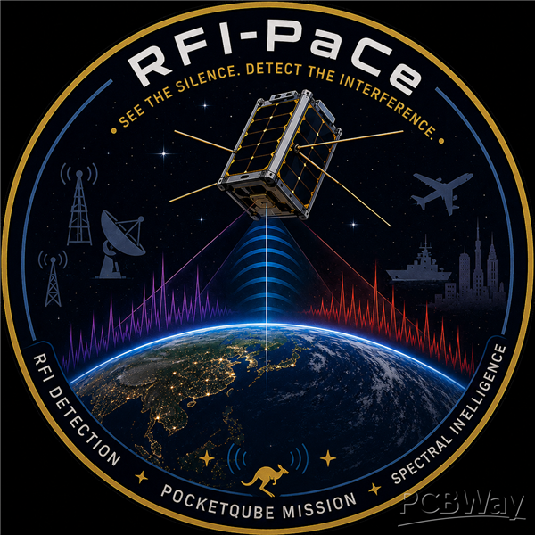
RFI-PaCe is a student team formed in January 2026 and selected as Team Australia for the 6th IEEE GRSS Student Grand Challenge, an international competition run by the IEEE Geoscience and Remote Sensing Society. A seven-student team from Griffith University and the University of Queensland, selected as Team Australia for the 6th IEEE GRSS Student Grand Challenge, building a dual-band (X and K) PocketQube-class payload that detects, characterizes and maps radio-frequency interference from orbit.
About us:
- Griffith University — four PhD candidates working in RF and microwave engineering, quantum physics, sports sensing, and computer science / IT, plus two undergraduate engineering students.
- University of Queensland — one student in IT and astrophysics.
The Problem:
Passive microwave observations are how we measure soil moisture, sea-surface salinity, sea ice and atmospheric water vapor from space. Those measurements sit in protected bands, and they are being corrupted by radio-frequency interference. RFI is invisible to the instruments it damages. A radiometer reports a brightness temperature, it cannot tell you that the number is wrong because a radar 400 km below was illuminating the same channel. Ground-based monitoring cannot see it either, because it does not see what a satellite sees.
The Mission:
RFI-PaCe is a PocketQube-class payload carrying separate X-band and K-band antennas with sub-patch elements.
The Payload:
- Detects RF energy in the 10.6–10.7 GHz and 18.6–18.7 GHz bands
- Characterizes it on-board — bandwidth, duty cycle, modulation signature, power
- Maps it by tagging every detection with the satellite's position and downlinking a compact feature record rather than raw IQ
That last point is the design driver. A PocketQube has a downlink budget measured in kilobytes, so the interesting engineering is in doing the signal processing on orbit and sending down a database entry instead of a waveform. The end product is an open-science RFI map that the passive-microwave community can actually use.
What we are building right now:
The first RF hardware iteration. Before anything flies, the receive chain has to be built and measured on the bench. We have split the full dual-band superheterodyne receiver into five separate test PCBs, so each stage can be characterized on its own before the chain is integrated onto flight-representative boards. Every board is designed on Rogers RT/duroid 5880 with SMA-launched, conductor-backed coplanar-waveguide interconnects so stages can be cascaded in any order on the bench.
The five boards follow the signal, antenna to ADC:
1 — RF front end (antenna input):
Two independent receive chains, one per band. Each takes the antenna feed, amplifies it with a low-noise front end and rejects out-of-band energy before anything else touches the signal. This board sets the system noise figure, so it is the one we most need to measure rather than trust.
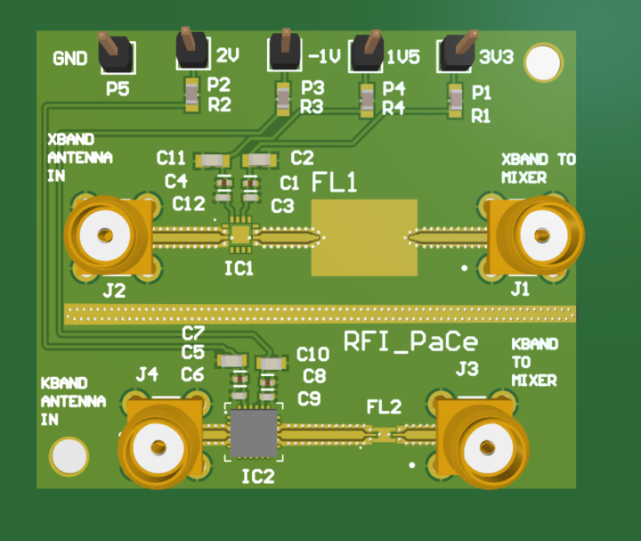
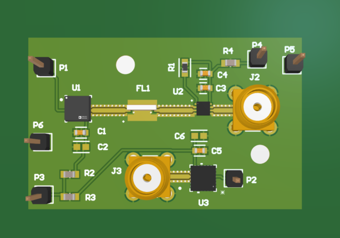
2 — Local-oscillator source board (free-running):
Generates the reference tone each band is mixed against. Built free-running first, so the oscillator tuning range and output power can be characterised on their own before the control loop is added.
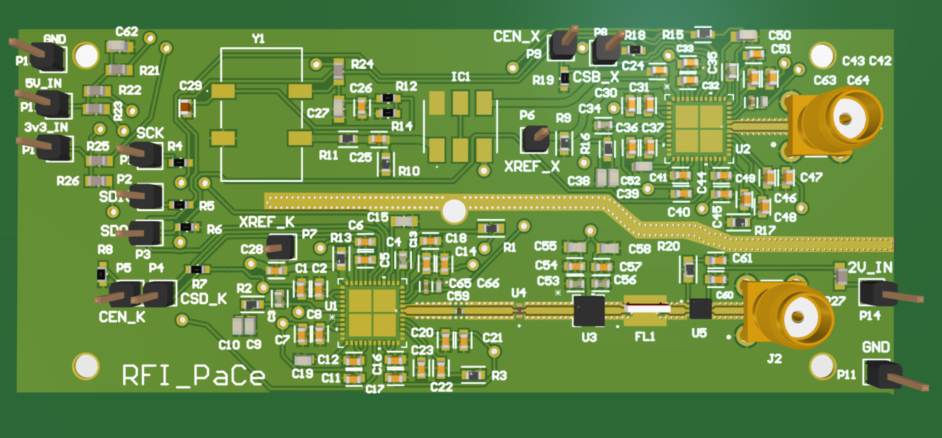
3 — PLL synthesizer board (locked LO):
This is our back up for if the the VCO board output can't stay reliable with change of temperature. This is less desirable as the PLL has a much higher power consuption. The same two oscillator chains, this time phase-locked to a crystal reference under SPI control. This is what turns a free-running oscillator into a frequency source stable enough for a radiometric measurement to mean anything.
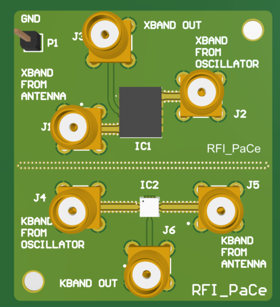
4 — Mixer board (down-conversion):
Down-converts each band against its own local oscillator to an intermediate frequency the digitiser can reach. Isolation between the LO, RF and IF ports is the parameter that decides whether this architecture works at all, and it is the reason this stage gets its own board.
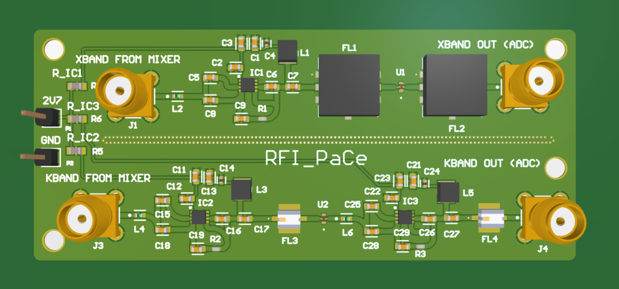
5 — IF gain and filter board (into the ADC):
Sets the pass-band and the signal level presented to the ADC — gain distribution, anti-alias filtering, and enough headroom that a strong interferer does not saturate the chain. Its output is the input to our ADC evaluation platform.
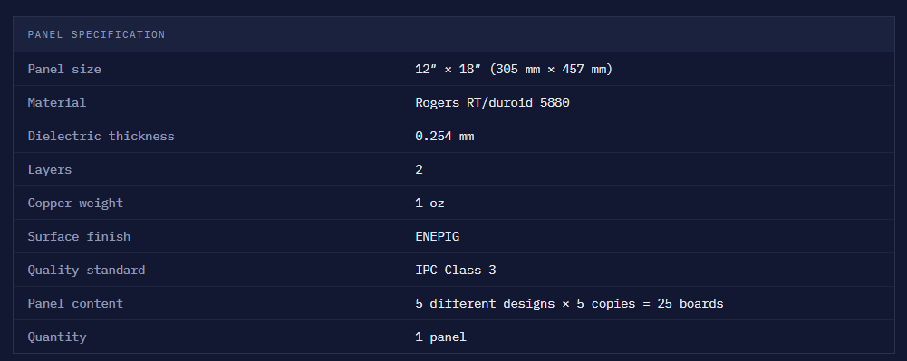
We are panelising five copies of each of the five designs — 25 boards — on a single 12" × 18" Rogers RT/duroid 5880 panel. Five copies is not over-ordering: at these frequencies we expect to iterate component values on the bench, we lose boards to destructive measurement and rework, several team members need to bring up stages in parallel, and we need known-good spares to demonstrate at our Critical Design Review.
We simulate before we fabricate:
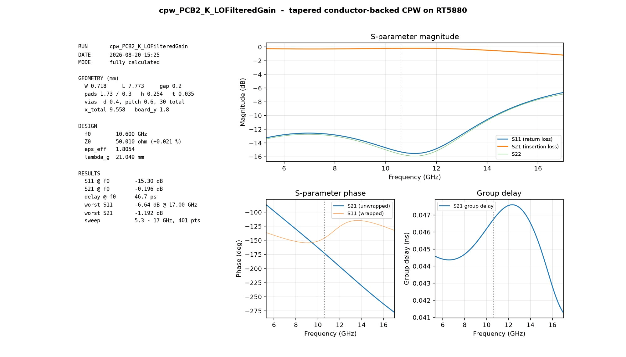
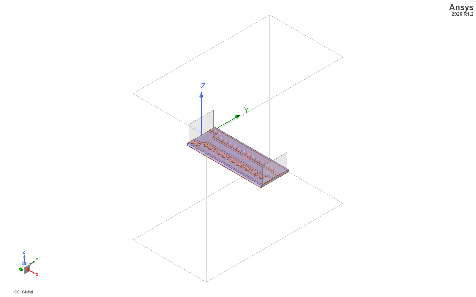
Every RF interconnect on these boards is simulated in Ansys HFSS (2026 R1.2) before release. As an example, the tapered conductor-backed CPW run on the LO board was solved across 5.3–17 GHz on 0.254 mm RT/duroid 5880:
Why Rogers RT/duroid 5880:
At 18.7 GHz, FR-4 is not a candidate. RT/duroid 5880 gives us Dk 2.20 with a dissipation factor of 0.0009 and, critically, the Dk stability that lets a simulated 50 Ω line still be a 50 Ω line on the bench. The 0.254 mm thickness keeps the CPW gap and via-fence pitch manufacturable while holding the substrate thin enough to suppress parallel-plate modes across K-band. It is also the material our flight antenna sub-patch array is designed on, so the test boards and the flight boards share a process.
What we are asking PCBWay for:
One fabricated 12" × 18" Rogers RT/duroid 5880 panel, free of charge.
We are sourcing and paying for all active and passive components ourselves — MMIC LNAs, mixers, VCOs, PLLs and filters are being sampled and purchased by the teams small budget. Fabrication on Rogers is the single largest line item we cannot cover, and it is the one that gates everything downstream: no boards, no measurements, no Critical Design Review.
Two questions we would appreciate an answer on:
- Is RT/duroid 5880 at 0.254 mm available through your standard Rogers stock, and what is the realistic lead time to Brisbane, Australia?
- Are you able to supply a solder-paste stencil for the panel? Several of the MMICs are fine-pitch QFN and DFN parts with ground paddles.
What PCBWay gets in return:
- Logo on the copper. Please feel free to put the PCBWay Logo on to any gap in the top overlay of all our boards.
- Logo on our competition material. PCBWay appears in the sponsor bar of our IEEE GRSS Student Grand Challenge poster, presentations and written submissions — material that is seen by the GRSS judging panel and the wider GRSS community, alongside our existing partners Ansys, LEAP Australia and PTC.
- A public build log. We post the project's progress on Instagram (@rfi_pace), and we will tag PCBWay consistently.
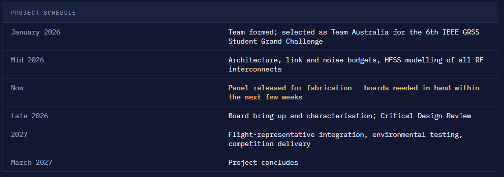
Timeline:
Contact:
Max Gadsby — Team Lead, RFI-PaCe (Team Australia) Griffith University, Brisbane, Australia
Email: max.gadsby@griffithuni.edu.au
Instagram: @rfi_pace
Apply for sponsorship >>- Comments(0)
- Likes(0)