PulsePhone
PulsePhone
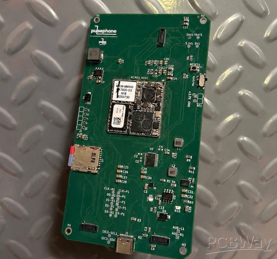
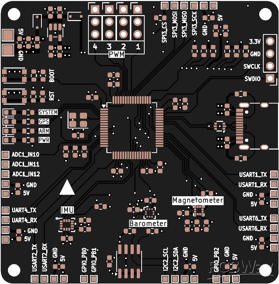
PulsePhone is an open source, modular Linux smartphone designed and built from the ground up by a single student engineer. The project's core idea is that a phone's most failure-prone and most desirable-to-upgrade components, the display, camera, radio, and battery, shouldn't be permanently soldered into the device. Instead, each of these is built as an independent, swappable module connected through a custom board-to-board interface standard called MBI-Lite, so any subsystem can be pulled and replaced without disassembling or redesigning the rest of the phone.
Who I am
I'm a self-taught student engineer (under 18), building PulsePhone entirely on my own, from schematic design through PCB layout, fabrication, and bringup. I design in KiCad, source and fabricate through JLCPCB, and do reflow and debugging work with support from a mentor. I taught myself hardware design, embedded Linux, and PCB layout specifically to make this project possible, and I treat it as a serious engineering effort, and not a hobby project, with staged bringup, schematic audits, and documented failures for each revision.
Architecture
The compute core is a Compulab i.MX93 system-on-module, chosen specifically to offload the hardest parts of the design, DDR memory routing, PMIC sequencing, and RF layout, work that isn't realistically achievable on a 4-layer board built by a solo engineer. The SoM carries a dual Cortex-A55 application processor alongside a Cortex-M33 microcontroller for low-power and real-time tasks. All peripheral modules attach through Hirose DF40 high-density board-to-board connectors, a 0.4mm pitch connector family typically used in compact high-reliability electronics, chosen for the module interface after evaluating it against alternatives like Panasonic's AXE/AXK series.
Revision process
Each board revision follows a consistent process: schematic design in KiCad, an internal audit pass focused on pin-level correctness, active-high vs active-low logic on every enable and reset pin, full power pin coverage, and pull-up/pull-down logic, followed by automated routing, then manual copper pour and ground plane fill, then design rule checking tuned to the fabricator's tolerances before the board is sent out.
Revision 1 served its purpose as a bringup learning board. Two significant issues surfaced during testing: the power regulator's enable pin was wired assuming active-high logic when the part was actually active-low, which collapsed the 3.3V rail on power-up, and the UART debug interface had a logic-level mismatch between the SoM's 1.8V I/O and the 3.3V/5V USB-to-serial adapter used for console access. A secondary issue was inconsistent LGA reflow quality from an early home-reflow attempt.
Revision 2 corrected all three: the regulator was replaced with a part whose enable pin ties directly to the input rail, removing the active-low failure mode entirely, the UART fix moves the logic-level translation to a dedicated 1.8V-capable USB-UART adapter rather than an onboard level shifter, and reflow for the compute module has been moved to a proper lab oven rather than a home setup, since LGA packages are highly sensitive to time-above-liquidus and reflow profile accuracy. Revision 2 also corrected a MIPI-CSI D0/D1 polarity swap found during schematic review. Bringup on Revision 2 follows a staged approach: verify the power tree rail-by-rail first, then bring up the UART console, then the bootloader, and only then attempt to boot with a display module attached, so that failures are isolated to the smallest possible stage rather than debugging a fully assembled system blind.
What's next
Revision 3 is planned to split the compute module itself onto a separate, swappable daughtercard connected via board-to-board connectors, conceptually similar to the Raspberry Pi Compute Module ecosystem. Because DDR routing stays internal to the SoM package, the daughtercard connector only needs to carry MIPI-CSI/DSI, USB, I2C, UART, and power, making it a tractable signal integrity problem rather than a full high-speed memory interface redesign. This would let the compute module be replaced if damaged, or upgraded to a GPU-capable SoM in the future, without needing to respin the entire main board.
On the software side, the target OS stack is a Wayland-based Linux environment, Phosh running on the phoc compositor, built through Yocto using Compulab's board support package layered with meta-wayland and meta-phosh. Since the i.MX93 has no GPU, the initial target uses software rendering (pixman), with the architecture designed so that a future GPU-capable compute module could drop in hardware-accelerated rendering with minimal changes above the compositor layer.
The full project, schematics, board files, and progress notes, is open source and public at https://github.com/pulseopen/PulsePhone/tree/dev.
Apply for sponsorship >>- Comments(0)
- Likes(1)