PYNQ Z2 Oscilloscope, Function Generator, Logic analyzer
This project started as a university minor project, but it quickly became something much more ambitious. I have always been highly interested in analog-to-digital converters, mixed-signal electronics, and the engineering that goes into measurement instruments such as oscilloscopes. At the same time, I had wanted for a long time to design a dense, high-performance multilayer PCB of my own rather than build another project around pre-made development modules. The PYNQ-Z2 Mixed-Signal Oscilloscope became an opportunity to combine both interests into a single system.
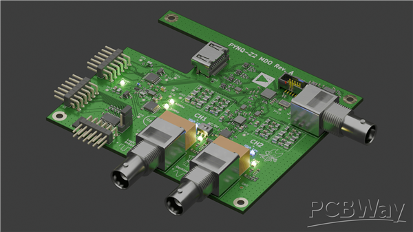
The objective was to design a complete mixed-signal acquisition platform around the PYNQ-Z2 FPGA board, with a custom four-layer PCB handling the analog front end, high-speed data conversion, clocking, signal generation, power conditioning, and the physical interface to the FPGA. Instead of treating the ADC as a black-box peripheral, I wanted to understand the entire signal path from the input connector to the digital samples entering the FPGA.
The analog input passes through a carefully designed front end before reaching the ADC. The circuitry provides signal conditioning and differential drive suitable for a high-speed converter. Particular attention had to be given to input impedance, gain, bandwidth, ADC common-mode requirements, protection, return-current paths, component parasitics, and the physical symmetry of the differential signal paths. The board also contains a DAC-based signal-generation path, allowing the same platform to function not only as an oscilloscope but also as a basic waveform-generation and mixed-signal experimentation platform.
The PCB itself became one of the largest parts of the project. I designed the schematic and four-layer PCB in KiCad, including controlled-impedance differential routing, analog and digital power distribution, ground-return planning, local decoupling, test points, via stitching, component placement, and high-density routing around the ADC, DAC, fully differential amplifiers, clocks, and the PYNQ-Z2 interface. I deliberately treated layout as part of the circuit rather than something performed after the schematic was finished.
Before committing the design to hardware, I performed extensive simulation and verification. Cadence PSpice was used for analog transient and frequency-domain simulations of the signal-conditioning circuitry. I tested the front end under multiple operating modes and frequencies to verify gain, settling behaviour, ADC input swing, and amplifier response.
MATLAB was then used to process exported simulation data and generate comparison plots for the different signal paths and operating configurations. This made it possible to compare the FDA output and ADC input quantitatively rather than relying only on visual inspection of simulation waveforms.
For PCB-level signal-integrity verification, I used Cadence Sigrity/PowerSI to analyse the routed interconnects and investigate the effects of the actual PCB geometry. This was particularly important because a schematic can be electrically correct while the fabricated implementation performs poorly due to transmission-line effects, return-path discontinuities, coupling, impedance variation, or poor placement. Differential-pair geometry, routing symmetry, reference planes, ground pours, and return-current paths were therefore checked as part of the design process.
The project required repeated iteration between simulation and PCB design. Component locations were adjusted, routing was refined, track widths were increased where appropriate, test points were repositioned, ground stitching was reviewed, sensitive analog areas were isolated, and small copper and keepout changes were made around critical amplifier and converter nodes. The final board is therefore the result of several schematic, simulation, PCB, and signal-integrity iterations rather than a single layout pass.
Component selection was another significant challenge. High-speed mixed-signal components are not always easily available or affordable for a student project. For several of the critical Analog Devices components, I contacted Analog Devices and obtained engineering samples directly from the manufacturer. That made it possible to design around genuine high-performance converter and analog components rather than replacing the architecture with lower-performance modules simply because they were easier to purchase.
The PYNQ-Z2 provides the digital side of the instrument. Its FPGA fabric provides the foundation for high-speed acquisition, timing, buffering, triggering, waveform generation, and future digital signal-processing functionality, while the Zynq processing system provides a path toward software control and visualization. This split between a custom mixed-signal PCB and an FPGA/processor platform was intentional: the PCB handles the analogue electrical problem, while the FPGA handles the deterministic high-speed digital problem.
A major lesson from the project was that building a measurement instrument is not just an ADC-selection problem. Performance depends on the complete chain: input network, amplifier noise and bandwidth, ADC drive requirements, reference and power integrity, clock quality, PCB stack-up, impedance control, grounding, return paths, FPGA timing, and signal processing. A problem in any one of these areas can dominate the entire system.
What began as a university minor project therefore became a much broader exercise in mixed-signal system design. It required KiCad for schematic capture and PCB layout, Cadence PSpice for circuit simulation, Cadence Sigrity/PowerSI for PCB-level signal-integrity analysis, MATLAB for simulation-data processing and visualization, and AMD/Xilinx PYNQ and FPGA tools for the digital acquisition platform. It also required component sourcing, manufacturer documentation, ECAD models, repeated design reviews, and several rounds of optimization before the board was ready for fabrication.
For me, the most important part of the project is that it is not simply an FPGA board connected to an ADC module. The analog front end, converter interface, waveform-generation path, power system, high-speed routing, and physical PCB implementation were designed specifically for this instrument. It represents the kind of project I originally wanted to build: a dense custom PCB where analog electronics, data converters, high-speed PCB design, simulation, and FPGA processing all have to work together as one system.
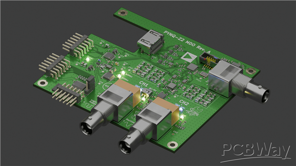
The images below show the progression from schematic design and circuit simulation to PCB layout, signal-integrity verification, and the final board design. The accompanying simulation plots and videos demonstrate the analogue front-end response, ADC drive signals, different acquisition configurations, and the behaviour of the complete mixed-signal signal path.
Apply for sponsorship >>- Comments(0)
- Likes(0)
 More by Engineer
-
 PYNQ Z2 Oscilloscope, Function Generator, Logic analyzer
This project started as a university minor project, but it quickly became something much more ambiti...
PYNQ Z2 Oscilloscope, Function Generator, Logic analyzer
This project started as a university minor project, but it quickly became something much more ambiti...
-
 PYNQ Z2 Oscilloscope, Function Generator, Logic analyzer
This project started as a university minor project, but it quickly became something much more ambiti...
PYNQ Z2 Oscilloscope, Function Generator, Logic analyzer
This project started as a university minor project, but it quickly became something much more ambiti...