OpenCalc - A cheaper and faster TI-84 style calculator
I’ve always been curious about computers but had only ever did firmware and never hardware, so I took it upon myself to self learn as much as I could about computer engineering and PCB design. Along with that, I noticed how ridiculously expensive the TI-84 calculators were and decided I could make a better, faster, cheaper one. So that’s what I did. This product is a proof of concept that a better and cheaper version of an overpriced produc can be made.
I wrote many thousands of lines of code and spent the last 3 months designing my first ever PCB. But when I went to order it, it was definitely outside of my price range. The whole project is open source on GitHub but I don’t currently have anywhere else to promote it. The project has also motivated me to take on an computer engineering minor at my university.
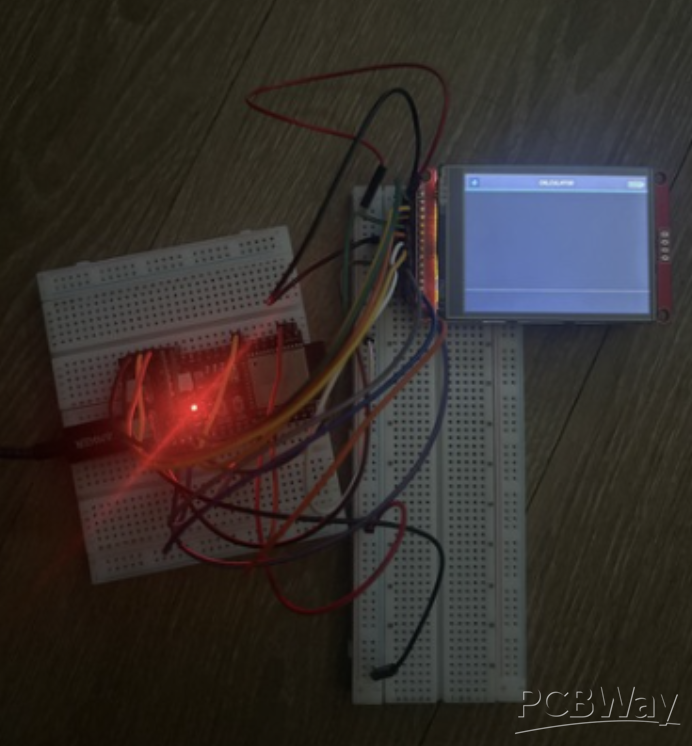
I decided to call it OpenCalc, since the whole thing is open sourced on github (https://github.com/CoryPearl/opencalc/tree/main), and the OpenCalc Os fully works (needs a few more tests) but is ready to be tested on really hardware not just a breadboard. I am hoping to be helped in the manufacturing of this project to get a start to my first ever finished computer engeneering project!
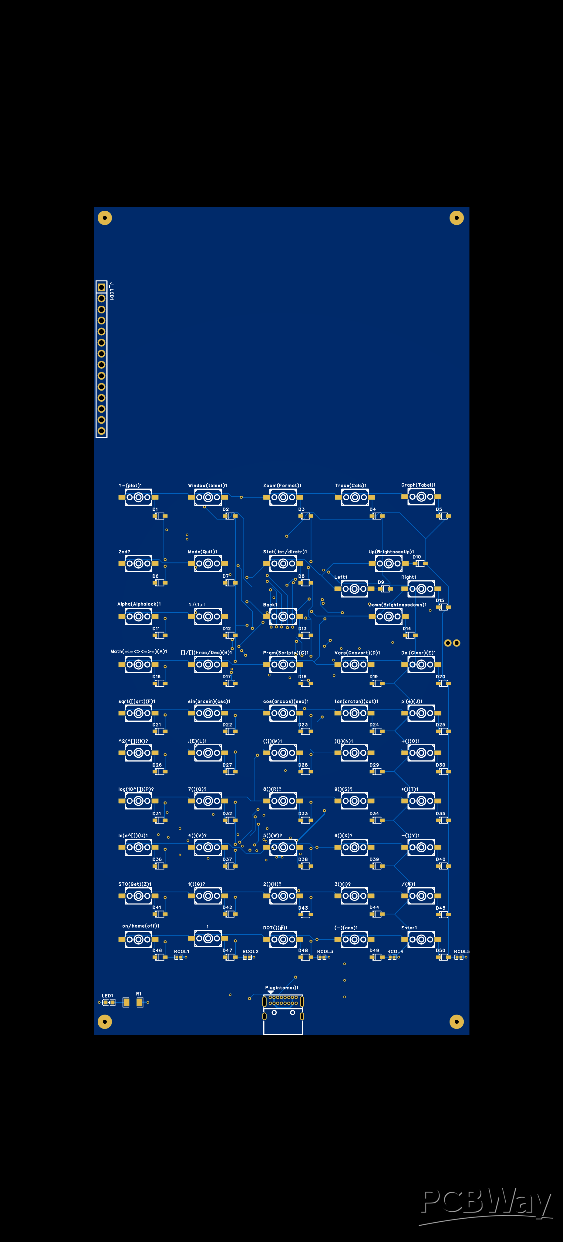
OpenCalc PCB — General Overview
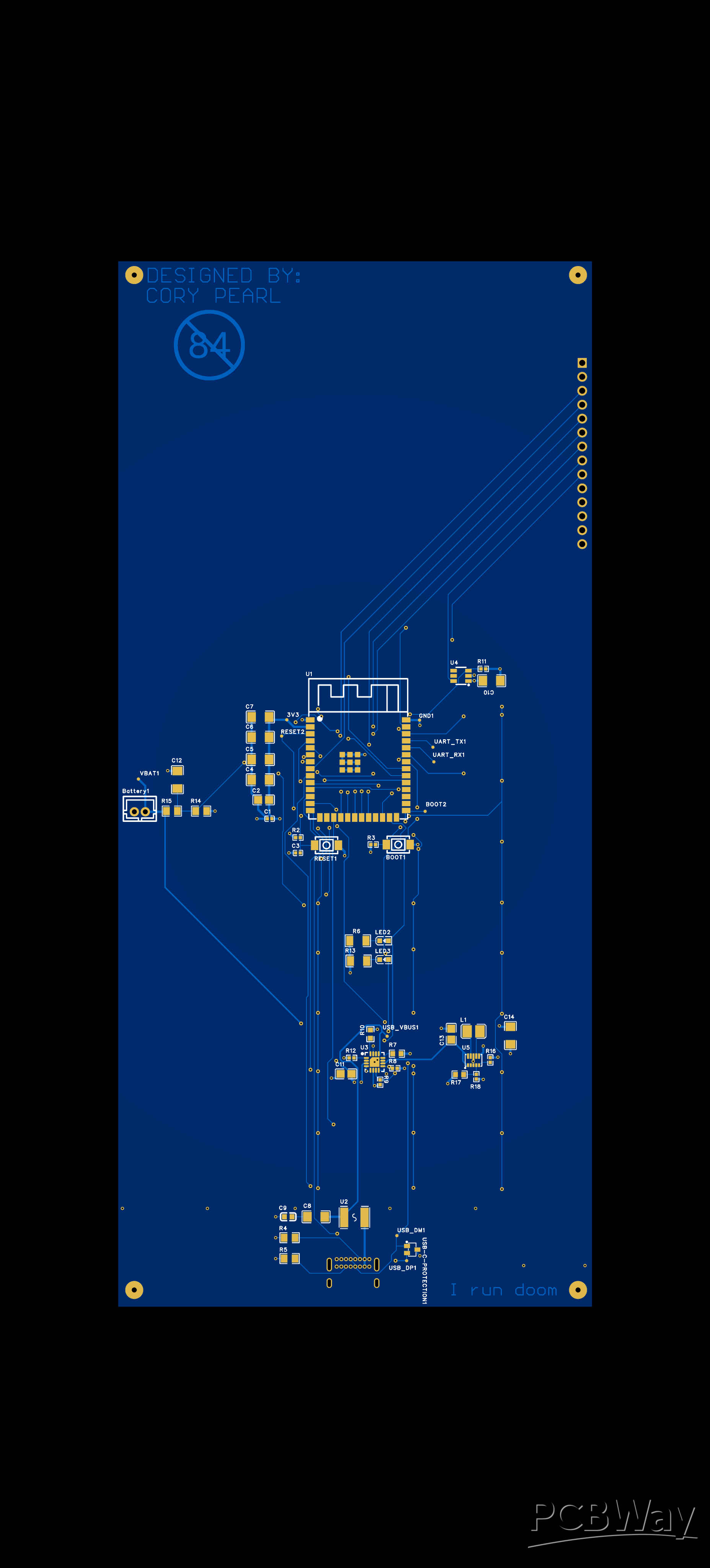
A plain-language summary of what's actually on this board, based on the V4 pcb.
Brain
- ESP32-S3-WROOM-1-N16R8 (16 MB flash, 8 MB PSRAM), with standard decoupling
capacitors.
- A power-on indicator LED (LED1) that's always lit whenever 3.3 V is present.
- Separate reset and boot buttons, each with its own pull-up resistor. Reset
also has a 1 µF debounce cap; boot doesn't.
Power Path
USB-C receptacle → single polyfuse on VBUS → BQ24074 LiPo charger (charges
the battery and produces a VSYS rail) → TPS63802 buck-boost regulator →
regulated 3.3 V rail.
- Two status LEDs come off the charger: a green one for "charging" and a
blue one for "power good," each with its own pull-up and series resistor.
- A simple resistor divider (two 1 MΩ resistors) halves the battery voltage
so it can be read on an ESP32 ADC pin.
USB-C
- Standard CC1/CC2 5.1 kΩ pulldowns.
- A small ESD protection chip (TPD2E2U06DCKR) sits between the connector's
D+/D− lines and the ESP32's native USB pins.
- Only VBUS is fused — D+/D− are not individually fused.
Display
- A 14-pin, 2.54 mm header wired for an ILI9341 SPI display: power, GND, CS,
RST, DC, MOSI, SCLK, MISO, and a backlight line.
- The backlight is switched by a small load-switch IC (TPS22918) rather than
a plain transistor, gated by a PWM signal from the ESP32 with a pulldown to
keep it off by default.
- The last 5 pins on that header — the ones that would carry touchscreen
signals — are left unconnected. As drawn, there's no touch support.
Keypad
- A 10-row × 5-column scan matrix, 50 keys total.
- Each key has its own series diode (anode toward the column, cathode toward
the row) to prevent ghosting on multi-key presses.
- Each column has its own 10 kΩ pull-up to 3.3 V.
- The ON/HOME key sits in the matrix like any other key, on the column used
for waking from sleep.
Battery
- 3.7 V 2000 mAh LiPo pack (103454 form factor), connecting through a 2-pin
JST-PHR connector.
- No separate protection circuitry is shown on the board itself — that would
need to live in the battery pack.
Test Points
Ten labeled probe pads: 3V3, GND, VBAT, USB_VBUS, RESET, BOOT, UART_TX,
UART_RX, USB_DP, and USB_DM.
Worth Flagging
There's no debug/expansion header, no power-hold/latch circuit, and no spare
GPIO breakout anywhere on this sheet. If these were expected from an earlier
version of the design, they've been dropped (or never made it into this
schematic).
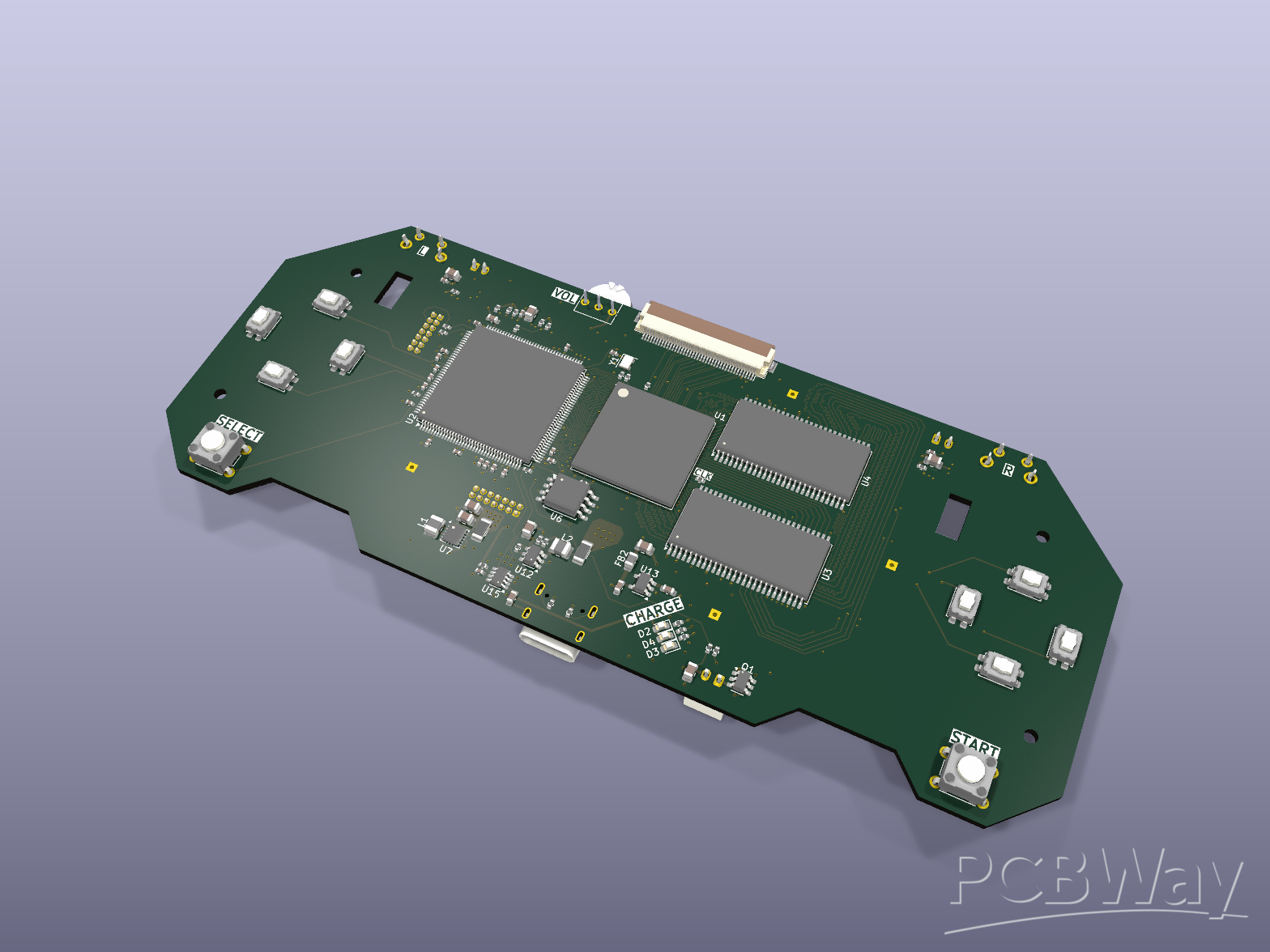
Front of board:
Back of board:
- Comments(0)
- Likes(0)