

ESP32 Smart Visitor Counter & Energy Saver
PROJECT TITLE
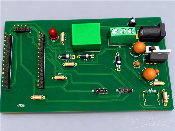
Compact Double-Sided ESP32 Smart Visitor Counter & Automatic Room Light Controller (KiCad PCB, 121 × 66 mm)
SHORT SUMMARY (one-liner)
A fabrication-ready double-sided PCB that counts people entering and leaving a room using two IR sensors, shows the live count on an OLED, and switches the room light automatically through a relay, powered by 12 V DC or USB-C.
TAGS
ESP32, KiCad, PCB Design, IR Sensor, Visitor Counter, Relay, OLED, Home Automation, Double-Sided PCB, Ground Plane, Gerber, L7805, USB-C, IoT
STEP 0: Project Overview
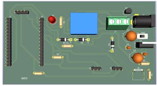
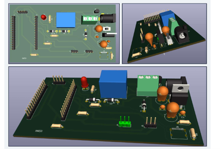
Automatic control of lighting is one of the simplest and most effective ways to reduce wasted electrical energy in classrooms, offices, laboratories and homes. A light left on in an empty room is a common source of avoidable consumption. This project solves that with a visitor-counting controller: it keeps track of how many people are inside and switches the load only when the count is greater than zero.
A circuit like this can be built on a breadboard or perfboard, but a properly designed PCB is what turns a prototype into a reliable product. This project therefore focuses not only on what the circuit does, but on how it is physically realised using modern PCB design practices.
Project at a glance
Board size: 121 mm × 66 mm
Layers: 2 (F.Cu signal layer + B.Cu solid ground plane), 1.6 mm FR-4, 1 oz copper
Controller: ESP32 development board (30-pin, plugs into female headers)
Sensing: 2 × IR proximity sensors (direction detection)
Display: I²C OLED
Output: 5 V SPDT relay driven by a BC547 transistor, with a 3-pin screw terminal for the load
Power: 12 V DC barrel jack or power-only USB-C
Regulation: L7805 with bulk and bypass capacitors
Design tool: KiCad 10 (Schematic Editor, PCB Editor, 3D Viewer)
Verification: DRC: 0 errors, 0 unconnected items
Outputs: Gerber (RS-274X), Excellon drill files, BOM, 3D views
STEP 1: Problem Statement and Objectives
Problem statement: To design a compact, reliable and manufacturable double-sided PCB for an automatic room light controller that counts visitors entering and leaving through a doorway using two IR sensors, displays the count on an OLED, and switches a light through a relay, while following industry-standard PCB design rules and generating complete fabrication-ready output files.
Objectives
Design the complete schematic of the visitor counter and light controller in KiCad.
Select suitable components and assign verified footprints.
Create a compact 121 mm × 66 mm double-sided layout with section-wise placement.
Provide a solid ground plane on the bottom layer, with thermal relief and ground-via stitching, for noise immunity.
Use trace widths well above the current-carrying requirement and route with manufacturable clearances.
Achieve a clean Design Rule Check with zero errors and zero unconnected items.
Generate Gerber layers, Excellon drill files, BOM and 3D views for fabrication.
Scope: schematic capture, footprint assignment, board outline, placement, routing, copper-zone design, ERC/DRC verification, 3D inspection and fabrication outputs. The relay isolates the switched load from the control electronics through its contacts, which are brought out on a three-pin screw terminal. Firmware and enclosure design are listed as future work.
STEP 2: Why Modern PCB Design Practices?
Older hand-drawn or single-sided layouts often suffered from long return paths, jumper wires, poor grounding and inconsistent clearances. Modern practice treats the PCB as an engineered component of the system:
Noise immunity: a continuous ground plane gives low-impedance return paths and shields signals.
Reliability: thermal relief and correct annular rings prevent soldering defects and weak joints.
Manufacturability: design rules matched to fabricator capability reduce rejected boards.
Compactness: two copper layers and optimised vias allow dense, tidy routing.
Verification: ERC and DRC catch errors before money is spent on fabrication.
STEP 3: System Overview and B
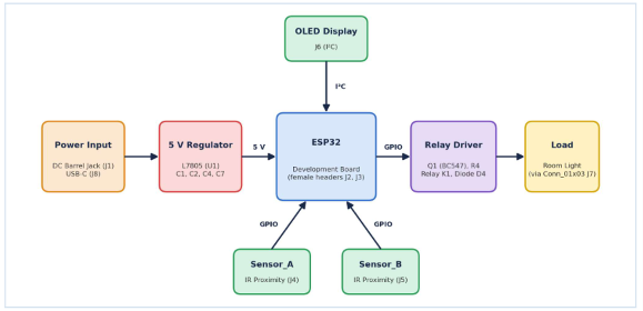
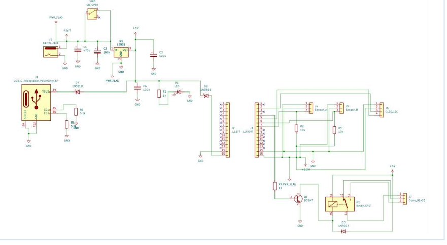
lock Diagram The controller monitors a doorway with two IR proximity sensors, Sensor_A and Sensor_B, mounted a short distance apart along the direction of passage. The order in which they are interrupted tells whether a person is entering or leaving. The ESP32 processes these events, maintains the count, updates the OLED and controls the light relay.
Functional blocks
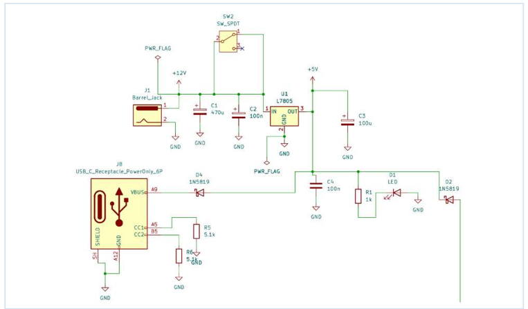
Power input: 12 V DC barrel jack (J1) with slide switch SW2, or the power-only USB-C connector (J8).
5 V regulator: L7805 (U1) with filter capacitors C1–C4 generates the 5 V rail; Schottky diode D4 (1N5819) lets USB VBUS feed the same rail.
Processing: ESP32 development board plugged into two 1×15 female headers, J2 (J_LEFT) and J3 (J_RIGHT).
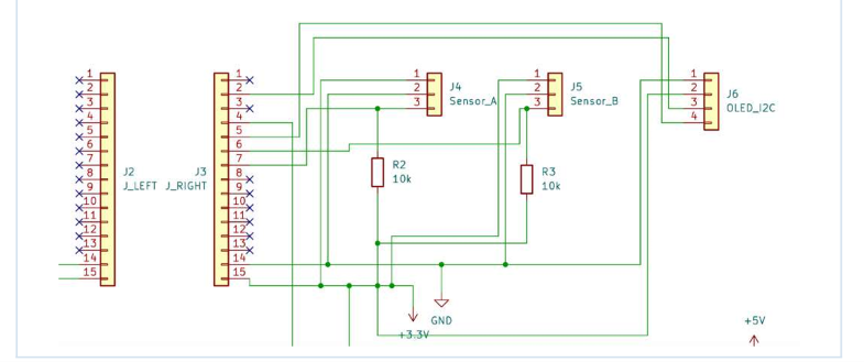
Sensing: two IR proximity sensors on 3-pin headers J4 (Sensor_A) and J5 (Sensor_B), with 10 kΩ pull-up resistors R2 and R3.
Display: I²C OLED on 4-pin header J6.
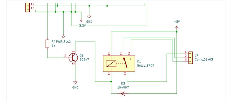
Load control: BC547 transistor Q1 with base resistor R4 drives relay K1; D3 (1N4007) is the flyback diode; the relay contacts go to 3-pin screw terminal J7.
STEP 4: Working Principle
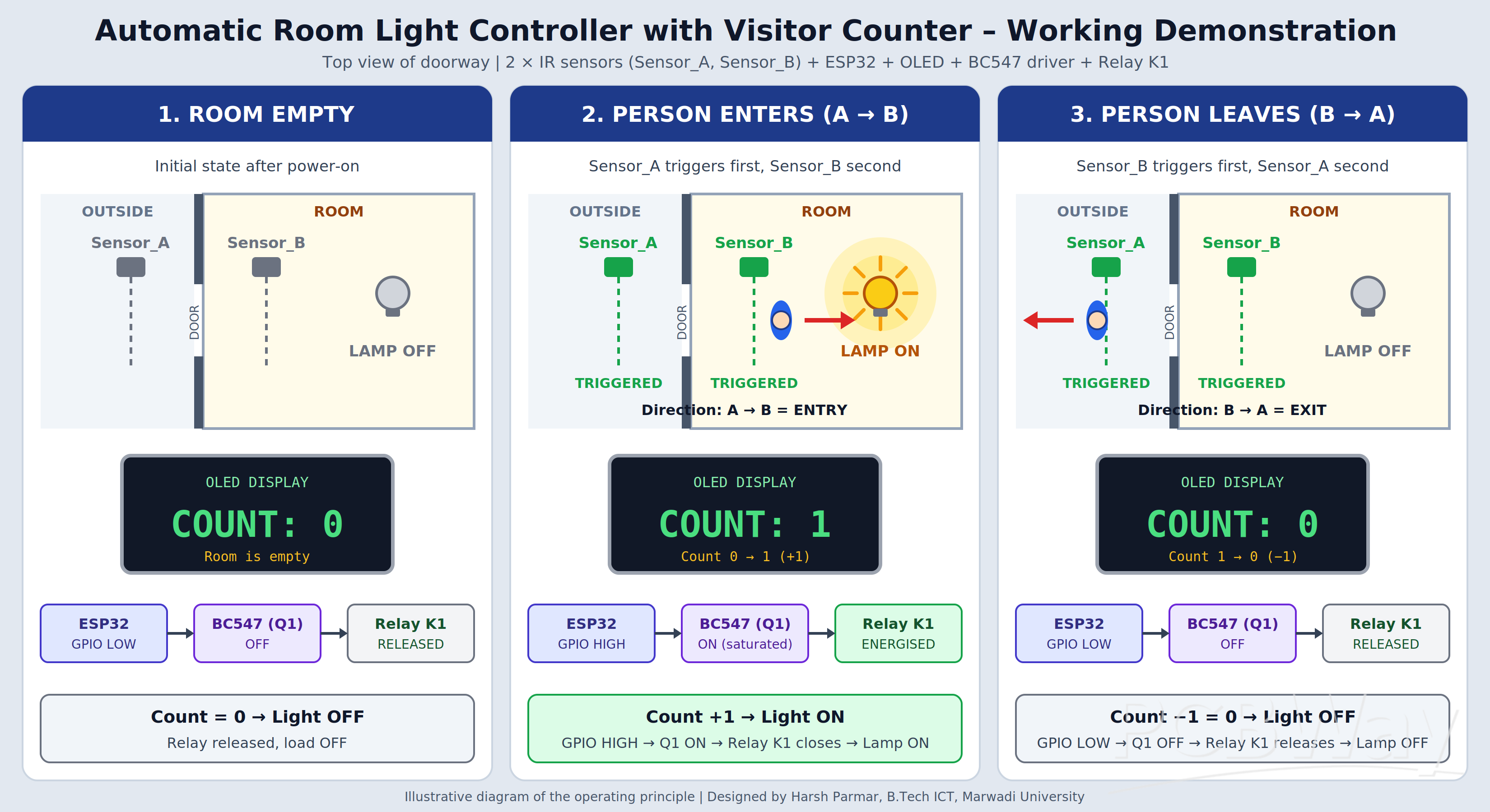
4.1 Direction detection: When a person enters, they interrupt Sensor_A first and Sensor_B second; when leaving, the order is reversed. The firmware records which sensor triggered first and increments the counter for A→B (entry) or decrements it for B→A (exit). A short debounce delay and a timeout between the two events prevent false counts.
4.2 Counting and display: The ESP32 holds the occupancy count in memory and never lets it fall below zero. After every valid event the count is refreshed on the OLED over I²C, so occupants and maintainers can see the room status at a glance.
4.3 Automatic light control: If the count is greater than zero, the ESP32 sets the control GPIO high. This saturates transistor Q1 through base resistor R4, energises the coil of relay K1 and closes its contacts, so the connected light turns ON. When the count returns to zero, the GPIO goes low, Q1 turns off and the relay releases. Diode D3 across the coil absorbs the inductive voltage spike when the coil is de-energised.
4.4 Operating flow
Power is applied through J1 (with SW2 on) or J8; the 5 V rail stabilises and the ESP32 boots.
The count is initialised to zero and the relay is held off.
Sensor events are read continuously; direction is resolved from the order of triggering.
The count is updated and shown on the OLED.
The relay is energised if the count is above zero, otherwise it is released.
STEP 5: Hardware Components and Bill of Materials
Key components
ESP32 development board: dual-core 32-bit MCU with Wi-Fi and Bluetooth, many GPIOs, I²C support, 3.3 V logic; sockets into the board so it can be reused.
IR proximity sensors: low-cost, contactless detection of a person crossing the beam, with a simple digital output.
OLED (I²C): high-contrast, low-power display needing only four connections.
L7805: simple, robust 5 V regulation with thermal shutdown and short-circuit protection.
Relay K1 with driver Q1: a GPIO cannot drive a relay coil directly, so the BC547 acts as a switch; the contacts isolate the load from the logic.
USB-C (J8): power-only connector; 5.1 kΩ resistors R5 and R6 on CC1/CC2 let a USB-C source supply 5 V.
Why these components?
ComponentReason for selectionESP32 DevKitSufficient GPIOs, I²C support, 3.3 V logic and room for IoT or app expansion; widely available.L7805 (U1)Converts the 12 V adapter input to a stable 5 V for relay, sensors, OLED and ESP32.470 µF / 100 µF + 100 nF capacitorsBulk capacitors handle load transients; 100 nF ceramics bypass high-frequency noise at the regulator.BC547 (Q1) with R4 = 1 kΩHandles the relay coil current (about 70–90 mA) comfortably; low cost, TO-92 package.1N4007 (D3)Clamps the relay-coil back-EMF; 1 A rating gives ample margin.1N5819 (D2, D4)Schottky diodes have a low forward drop, so little voltage is lost on the 5 V path.SW2 and LED D1SW2 gives a manual power switch; D1 with R1 gives a power-on indication.Through-hole partsEasy hand soldering and inspection during prototyping and viva demonstration.
STEP 6: Schematic Design
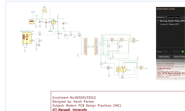
The schematic (project ESP32_Visitor_Counter, A3 sheet, revision 1.0) was drawn in KiCad’s Schematic Editor with functional blocks arranged logically: power input and regulation, ESP32 headers with sensors and OLED, and the relay output stage. Power rails (+12 V, +5 V, +3.3 V, GND) use power symbols, and PWR_FLAG symbols mark the driven power nets so the checker recognises them.
6.1 Power supply section
Power can be applied through barrel jack J1 or USB-C connector J8. On the 12 V path, slide switch SW2 connects the input to C1 (470 µF bulk) and C2 (100 nF bypass) ahead of regulator U1. The 5 V output is smoothed by C3 (100 µF) and C4 (100 nF). Schottky diode D4 connects USB VBUS (pin A9) to the 5 V rail, and resistors R5 and R6 (5.1 kΩ) on CC1 and CC2 identify the board as a USB-C power sink. LED D1 with R1 indicates that the rail is live, and D2 is a further 1N5819 Schottky diode on the 5 V branch.
6.2 Sensor and display interfacing
Sensor_A (J4) and Sensor_B (J5) are three-pin headers (VCC, GND, OUT). Their OUT lines are routed to ESP32 GPIO inputs on J2/J3 and held at a defined level by 10 kΩ resistors R2 and R3. The I²C OLED connects through header J6 (SDA, SCL, power, ground). Sensor and OLED headers sit near the board edge for short wiring to the doorway sensors and the display.
6.3 Output driving circuit
The ESP32 control GPIO connects to the base of NPN transistor Q1 (BC547) through R4 (1 kΩ). The emitter is grounded and the collector sinks the coil current of relay K1. Flyback diode D3 (1N4007) sits across the coil to suppress the voltage spike when the coil switches off, protecting Q1 and the neighbouring circuitry. The relay contacts are brought out to the three-pin screw terminal J7.
6.4 Footprint assignment
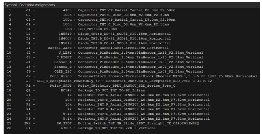
Each symbol was assigned a footprint using KiCad’s Footprint Assignment tool and the standard libraries (26 symbols). Pad sizes, drill diameters and pitches were compared with datasheet dimensions before layout began. USB-C connector J8 uses the HRO TYPE-C-31-M-12 footprint.
6.5 Electrical Rules Check (ERC)
ERC was run on the finished schematic to confirm that no pins are left unconnected, no power pins are undriven and no nets are shorted. The only message is a library warning that the Relay_SPDT symbol differs from its library copy; this concerns symbol graphics only and
STEP 7: PCB Layout Design
7.1 Why double-sided?
The top layer carries all signal routing, while the bottom layer is dedicated to an unbroken ground plane. Compared with a single-sided design this eliminates jumper wires, shortens return paths, reduces loop area and allows a smaller board. For a design combining an ESP32, an I²C display, a relay and a linear regulator, this gives clearly better noise performance and reliability.
7.2 Board outline and component placement
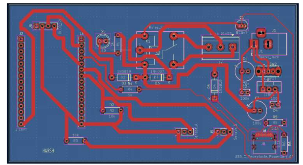
The outline was defined on the Edge.Cuts layer as 121 mm × 66 mm. Components were placed section-wise to keep functions separate and traces short:
Power section: J1, SW2, U1 and the filter capacitors on the right side, together with J8, so high-current paths and regulator heat stay away from the logic.
ESP32 section: the two 1×15 headers J2 and J3 occupy the left and centre, giving short routes to all peripherals.
Relay section: K1, Q1, R4, D3 and screw terminal J7 are grouped at the top, away from the sensor lines.
Sensors and OLED: J4, J5 and J6 are placed along the board edges for easy cable access.
7.3 Design parameters
ParameterValueRemarkBoard size121 mm × 66 mmCompact form factorLayers2 (F.Cu, B.Cu)Double-sided, 1.6 mm FR-4Copper weight1 oz (35 µm)StandardTrace width≥ 1.0 mmWide routing on all nets, far above the current requirementMinimum clearance0.2 mmWithin standard fabricator capabilityVia size / drill0.8 mm / 0.4 mmStandard, low-cost drillGroundSolid GND zone on B.CuTop-side ground pads tied to it with GND vias
7.4 Ground plane design
A filled GND copper zone covers the whole bottom layer. Ground pads on the top layer connect to it through vias and thermal-relief connections. A continuous ground plane gives signals a nearby low-impedance return path, reduces loop area and EMI, and acts as a heat spreader around the regulator. Zone clearance was matched to the design rules so the fill never violates spacing to other nets.
7.5 Thermal relief
Through-hole pads connected to the ground pour use thermal-relief spokes rather than solid connections. The spokes limit heat conduction away from the pad during soldering, so the joint reaches soldering temperature and cold joints are avoided, while still giving a low-resistance electrical path in operation.
Regulator U1 deserves special attention. With a 12 V input and a load of roughly 0.25–0.3 A, the L7805 dissipates (12 V − 5 V) × I ≈ 1.8–2.1 W. A TO-220 package without a heat sink will run hot at this level, so U1 is surrounded by copper and a small clip-on heat sink is recommended. When the board is powered from USB-C the regulator is bypassed and dissipates nothing.
7.6 Trace width calculation (IPC-2221)
Trace widths were checked with the IPC-2221 relationship for external layers, I = k · ΔT^0.44 · A^0.725, where k = 0.048, ΔT is the temperature rise in °C and A is the cross-sectional area in mil². For 1 oz copper (about 1.38 mil thick) and a 10 °C rise:
Net typeTypical currentMin. calculated widthWidth usedSensor / I²C / GPIO signals< 20 mA< 0.1 mm≥ 1.0 mmRelay coil path (Q1, D3)≈ 80 mA≈ 0.1 mm≥ 1.0 mm5 V distribution≈ 0.3–0.5 A≈ 0.15–0.2 mm≥ 1.0 mmRelay contact / load pathup to 1 A≈ 0.3 mm≥ 1.0 mm
All nets are routed well above the calculated minimum. The generous width lowers voltage drop and temperature rise, makes the board tolerant of etching variation, and is easy to manufacture.
7.7 Routing strategy
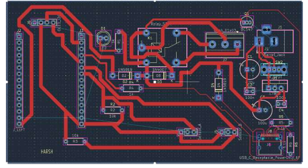
Routing was done interactively with 45° bends and short, direct paths. Power and relay-driver nets were routed first, followed by the sensor, display and ESP32 signal nets. Right-angle corners were avoided, and the relay-coil loop (K1, Q1, D3) was kept tight and apart from the sensor lines. All signal tracks are on the top layer, leaving the bottom layer free for an unbroken ground plane.
7.8 Via optimisation and ground stitching
Vias were kept at a standard 0.8 mm / 0.4 mm size so they stay inexpensive and reliable. After the first routing pass, 21 unconnected items appeared in the ratsnest. Analysis showed that the signal traces had divided the GND copper into small isolated islands, so ground could not reach every pad.
The fix was GND via stitching: ground vias were placed near the unconnected pads around C1, C2, the ESP32 headers, the sensors and the OLED, linking the top-side ground pads to the bottom ground plane. After refilling all zones, the unconnected count fell from 21 to 0. Stitching also reduces ground impedance, improves return-path continuity and strengthens shielding.
7.9 Signal integrity considerations
Short, direct signal traces keep inductance and coupling low.
The continuous ground plane gives every signal an adjacent return path.
The I²C lines to the OLED are routed together and kept away from the relay and regulator section.
Bypass capacitors C2 and C4 sit close to the regulator pins.
The relay coil and its flyback diode D3 form a tight loop, away from the sensor lines.
STEP 8: Issues Faced and How I Solved Them
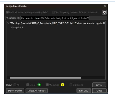
IssueCauseResolution“No net” errors on J8 (USB-C)Dual-pad structure of the connector footprint left overlapping pads without a netAssigned unified nets: A12 to GND and A9 to VBUSNPTH hole clearance violationInteractive router passed a trace over a mounting hole of the USB-C connectorChanged router mode to “Walk around” and re-routed along a safe path21 unconnected itemsSignal traces split the GND pour into isolated islandsPlaced GND stitching vias and refilled zones: result 0 unconnectedLibrary mismatch warning (J8)Footprint was edited locally and differs from the library copyVerified geometry manually; the warning does not affect manufacturingRemaining signal connectionsR4–Q1 base and the last diode pins were still openRouted manually and re-ran DRC
STEP 9: Design Rule Check (DRC)
The DRC covers clearance, track width, via size, annular ring, hole-to-hole spacing, board-edge clearance, silkscreen overlap and unconnected items.
CheckResultErrors0Unconnected items0Warnings1 (library footprint mismatch on J8, safe for manufacturing)
STEP 10: Manufacturing Considerations and 3D View
Clearance: 0.2 mm minimum copper clearance, within typical low-cost fabricator limits.
Annular ring and drill: pads and vias are sized to keep an adequate annular ring after drilling tolerance.
Solder mask: openings follow the pad shapes with a small expansion.
Silkscreen: reference designators and polarity marks are kept clear of pads; the name “HARSH” is added on F.Silkscreen.
Board edge: copper and components are kept clear of the Edge.Cuts outline.
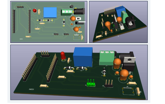
The KiCad 3D Viewer was used to inspect component placement, connector orientation, board outline and silkscreen, and to confirm that no parts collide or overhang the board edge.
STEP 11: Fabrication Files and Gerber Generation
The fabrication package was produced from KiCad’s Plot dialog (Gerber, RS-274X) and the Generate Drill Files dialog (Excellon). All files carry the prefix ESP32_Visitor_Counter. Each layer was then opened in the KiCad Gerber Viewer to confirm the output.
Readiness for fabrication: the DRC shows zero errors and zero unconnected items, all copper, mask, silkscreen, paste, outline and drill files are present, minimum clearances and sizes lie within standard fabricator capability, and the Gerber Viewer check confirms every layer was exported correctly. All Gerber and drill files are supplied as a ZIP together with the source project and BOM.
STEP 12: Testing and Validation
Design verification (done):
ERC on the schematic: no connection errors, one library-symbol warning for the relay.
DRC on the layout: 0 errors, 0 unconnected items, one footprint-library warning for J8.
3D views confirm component orientation and clearances.
Test procedure for the assembled board
Visual inspection: check for solder bridges, missing parts and correct polarity of C1, C3, D1–D4 and Q1.
Continuity test: confirm there is no short between 5 V and GND with a multimeter before applying power.
Power-up test: apply 12 V (SW2 on) and measure the regulator output; expected 5 V ± 5 %. Repeat via USB-C.
Sensor test: block each IR sensor and verify the output level changes.
Display test: confirm the OLED initialises and shows the count.
Direction test: pass an object A→B then B→A and observe the count.
Relay test: verify the relay clicks when the count is above 0 and releases at 0.
TestConditionExpected resultPower rail12 V via J1 (SW2 on) or 5 V via J85 V present on the 5 V rail; LED D1 onEntryA triggered, then BCount +1, light ONExitB triggered, then ACount −1, light OFF at 0Empty roomCount = 0Relay released, load OFFNegative guardExit event at count 0Count stays at 0Relay back-EMFRelay switched OFFNo stress on Q1; spike clamped by D3
Troubleshooting guide
No power: check J1 polarity, SW2 position, C1 orientation and regulator orientation.
ESP32 not booting: verify 5 V at the ESP32 VIN pin and that the board is seated correctly in J2/J3.
Wrong count direction: swap the Sensor_A and Sensor_B assignment in firmware.
False counts: adjust sensor sensitivity and the debounce interval.
Relay does not switch: check Q1 orientation, R4 value and the 5 V coil supply.
Regulator hot: add a heat sink to U1 or power the board from USB-C.
STEP 13: Results and Discussion
Achievements
Complete schematic and double-sided PCB designed in KiCad (project ESP32_Visitor_Counter).
Compact 121 mm × 66 mm board with section-wise placement.
Final DRC result: 0 errors and 0 unconnected items.
Solid ground plane on the bottom layer, stitched to the top-side ground pads with vias; 21 initial unconnected items resolved.
USB-C footprint and routing issues diagnosed and fixed.
Gerber layers, Excellon drill files, BOM and 3D views generated.
Impact of modern practices: the bottom-layer ground plane and via stitching provide continuous return paths and reduce noise; thermal-relief connections make soldering reliable; generous trace widths avoid overheating; DRC removed layout errors before fabrication; and section-wise placement kept routing short and clean. Together these give a board that is more reliable and easier to manufacture than an informally drawn layout.
Single-sided vs this design
AspectSingle-sided / older practiceThis design (modern)Routing layers1, jumper wires needed2 layers, no jumpersGroundingThin ground tracesSolid ground plane on bottom layer, stitchedNoise immunityPoor, long return pathsGood, short return pathsSoldering reliabilitySolid pad-to-copper joinsThermal-relief padsVerificationVisual onlyERC + DRC with 0 errorsFabrication outputManual artworkGerber + Excellon, ready to send
Limitations: the L7805 is a linear regulator and dissipates heat in proportion to the input-output voltage difference, so on a 12 V input it needs a heat sink; a buck converter would be more efficient. IR sensors may be affected by strong ambient light, and the relay contact rating must be respected for the connected load. The board has been verified by ERC and DRC; functional test results will be added once the assembled board is tested.
STEP 14: Conclusion and Future Scope
Conclusion: this project designed a compact double-sided PCB for an Automatic Room Light Controller with Visitor Counter, covering the full flow from schematic capture and footprint assignment through placement, routing, ground-plane design, DRC, 3D inspection and Gerber/drill generation. Real design problems, namely the USB-C footprint nets, a router hole violation and isolated ground islands, were identified and resolved with sound engineering methods, leading to a final DRC result of zero errors and zero unconnected items. The design is ready to be fabricated and assembled.
Future scope
Replace the L7805 with a buck converter for higher efficiency.
Add a Wi-Fi dashboard or mobile app for remote occupancy monitoring using the ESP32.
Use a solid-state relay or optocoupler-isolated driver for quieter, isolated switching.
Add ambient-light sensing so lights switch on only when needed.
Add an RTC and data logging for occupancy analytics.
Design a custom enclosure and move to SMD components for a smaller, production-grade board.
Add a mains-rated section with proper creepage and slots if switching mains loads directly.
STEP 16: References
KiCad EDA, “KiCad 10 Documentation: Schematic Editor and PCB Editor”, https://docs.kicad.org
IPC-2221B, “Generic Standard on Printed Board Design”, IPC, 2012.
Espressif Systems, “ESP32 Series Datasheet”.
STMicroelectronics, “L78 Series Positive Voltage Regulators Datasheet (L7805)”.
ON Semiconductor, “BC546/547/548 NPN Epitaxial Silicon Transistor Datasheet”.
Vishay, “1N5819 Schottky Barrier Rectifier Datasheet” and “1N4001–1N4007 General Purpose Rectifiers Datasheet”.
Ningbo Songle Relay, “SRD Series 5 V Relay Datasheet”.
USB Implementers Forum, “Universal Serial Bus Type-C Cable and Connector Specification”.
H. W. Johnson and M. Graham, High-Speed Digital Design: A Handbook of Black Magic, Prentice Hall, 1993.
H. W. Ott, Electromagnetic Compatibility Engineering, Wiley, 2009.
R. S. Khandpur, Printed Circuit Boards: Design, Fabrication, Assembly and Testing, Tata McGraw-Hill, 2005.
Designed by Harsh Parmar | B.Tech ICT, Marwadi University, Rajkot
- Comments(0)
- Likes(1)