May 14,2019
2,064 views
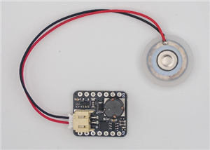
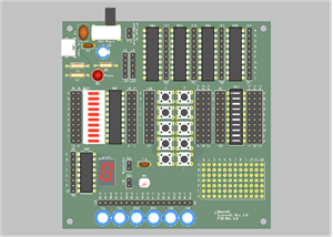
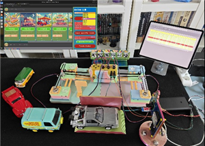
Power Bank circuit
2 Layers PCB 67 x 68.7 mm FR-4, 1.6 mm, 1, HASL with lead, Blue Solder Mask, White silkscreen
2064
2
0
10.00 (1)
Published: May 14,2019
Standard PCB
Download Gerber file 21
PCBWay Donate 10% cost To Author
Only PCB
*PCBWay community is a sharing platform. We are not responsible for any design issues and parameter issues (board thickness, surface finish, etc.) you choose.


Under the
Attribution-ShareAlike (CC BY-SA)
License.


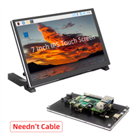
Raspberry Pi 5 7 Inch Touch Screen IPS 1024x600 HD LCD HDMI-compatible Display for RPI 4B 3B+ OPI 5 AIDA64 PC Secondary Screen(Without Speaker)
BUY NOW


- Comments(0)
- Likes(2)
Upload photo
You can only upload 5 files in total. Each file cannot exceed 2MB. Supports JPG, JPEG, GIF, PNG, BMP
0 / 10000
VOTING
1 votes
- 1 USER VOTES
10.00
- YOUR VOTE 0.00 0.00

-
10design
-
10usability
-
10creativity
-
10content
10.00
You may also like
-
Programmable Mist Maker - XIAO / QT PY Extension
830 1 0 -
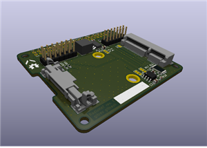
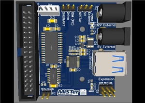
RadioHAT - Raspberry Pi radio development platform
670 0 2 -
-
-
-
-
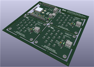
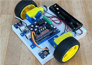
ARPS-2 – Arduino-Compatible Robot Project Shield for Arduino UNO
3130 0 6 -
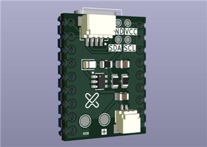
A Compact Charging Breakout Board For Waveshare ESP32-C3
3756 3 8 -
AI-driven LoRa & LLM-enabled Kiosk & Food Delivery System
4084 2 2