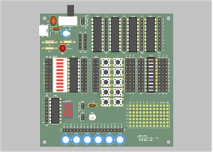
74HC595 Breakout Board
The stock 74HC595 has a very unintuitive layout. The output pins are on different sides of the boards, which makes routing more of a hassle than it needs to be. I designed a breakout board to get around this issue.
VCC is pin 1, and is next to SRCLR on pin 2. I did this since you typically tie SRCLR high. Output enable is on pin 7 and is next to ground (pin 8), since you also typically tie output enable low. In between are SRCLK, RCLK, SER IN, and SER OUT. On the right side, from pin 16 and working your way down is outputs A through H.
Holes for an optional power supply filter capacitor are included if you want to filter transients and ripples.
This design is a more intuitive approach than the stock chip pinout. Enjoy!
74HC595 Breakout Board
*PCBWay community is a sharing platform. We are not responsible for any design issues and parameter issues (board thickness, surface finish, etc.) you choose.


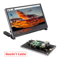
Raspberry Pi 5 7 Inch Touch Screen IPS 1024x600 HD LCD HDMI-compatible Display for RPI 4B 3B+ OPI 5 AIDA64 PC Secondary Screen(Without Speaker)
BUY NOW


- Comments(0)
- Likes(0)
More by Gregory Gavarian
-
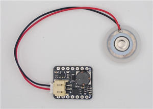
Programmable Mist Maker - XIAO / QT PY Extension
450 0 0 -
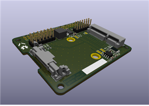
RadioHAT - Raspberry Pi radio development platform
359 0 1 -
-
-
-
-
ARPS-2 – Arduino-Compatible Robot Project Shield for Arduino UNO
2899 0 6 -
A Compact Charging Breakout Board For Waveshare ESP32-C3
3402 3 8 -
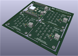
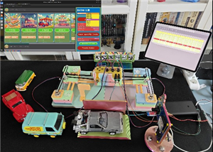
AI-driven LoRa & LLM-enabled Kiosk & Food Delivery System
3727 2 2