
|
LT Spice |
|

|
KiCad 9.0 |
|
|
|
PDN toolRolf V. Ostergaard
|
Mercury Rev 1 — GPU-Class High-Current Power Delivery Test Board
What is your project about?
Mercury (GPU) Rev 1 is a GPU-class power delivery and load-emulation board designed to explore the electrical, mechanical, and layout challenges found in modern graphics cards and high-performance compute hardware.
The project represents a deliberate first step toward working in the GPU and power-delivery industry. Rather than building a generic power supply or a simplified demonstration circuit, Mercury focuses on designing the type of system actually used on real GPU boards — a high-current, low-impedance VCORE power delivery network capable of supporting fast, large transient loads.
Instead of implementing a functional GPU, the design isolates and studies the power system itself, including:
multi-phase VRM architecture,
decoupling hierarchy and placement,
current return paths and plane geometry,
and transient load response under realistic conditions.
By pairing the VRM with a programmable MOSFET load bank, the board allows GPU-like power behaviour to be analysed without requiring proprietary silicon. This makes it possible to study real-world power integrity trade-offs in a controlled, repeatable, and manufacturable design.
Mercury is intended as both a learning platform and a professional portfolio project, closely aligned with the type of power delivery work performed at companies such as AMD and NVIDIA.
Current capability and operating envelope
Mercury is designed to safely deliver and sink up to ~500 A of controlled load current on the VCORE rail, with current magnitude and slew rate governed by firmware. The multi-phase VRM, capacitor network, and load architecture are dimensioned to support large step loads while maintaining controlled voltage droop and stable operation.
While the absence of on-die capacitance prevents replication of the most extreme sub-nanosecond GPU transients, Mercury is capable of producing hundreds of amps of repeatable, programmable load steps that realistically stress the power delivery network across the frequency ranges that matter at the PCB level. This makes the platform well-suited for analysing transient response, current sharing, return-path behaviour, and layout effectiveness under GPU-class current levels.
Why did you decide to make it?
I decided to build this project to deliberately push my technical ability and to gain a deeper, practical understanding of GPU-class power delivery systems — an area I find both extremely challenging and genuinely fascinating.
Rather than copying existing designs at face value, my goal was to understand why certain design decisions are made in industry practice, and where the real trade-offs lie. This became especially clear when iterating from earlier revisions of the board to the current design. I learned that performance does not scale linearly with “more” — more phases, more capacitance, or larger components do not automatically result in better behaviour.
For example, it is easy to assume that adding large amounts of capacitance will always improve VCORE stability. In practice, this quickly leads to diminishing returns, while significantly increasing board area, cost, and complexity. Early revisions of the project used large 680 µF bulk capacitors because simplified PDN tools favoured them due to their low-frequency performance. However, after building simplified time-domain and AC models in LTspice, it became clear that for the frequency ranges that actually dominate transient droop, the performance difference between 680 µF and 330 µF capacitors was negligible — and in some cases the smaller SMD polymer capacitors provided better overall behaviour due to placement flexibility and lower effective inductance.
This shift in understanding directly influenced the current design, which replaces large through-hole bulk capacitors with SMD polymer devices more representative of modern GPU hardware.
Phase count was another deliberate compromise. While higher phase counts (such as 16-phase VRMs) are common in flagship GPUs, controller availability and NDA limitations required this design to use a 12-phase topology. Even so, a 12-phase VRM remains a serious power system, and the design still captures the electrical and layout challenges present in real products.
Finally, this project was motivated by direct industry feedback. An AMD recruiter highlighted that designing a power delivery system capable of handling ~500 A with less than 40 mV droop is both extremely challenging and highly relevant to real GPU power delivery teams. AMD and NVIDIA are my long-term career goals, and Mercury was built as a realistic, technically honest project aligned with that level of engineering work.
How does it work?
Mercury is powered from a 12 V input rail and implements a multi-phase VCORE power delivery system using discrete DrMOS power stages and external inductors. The design prioritises realistic current distribution, transient behaviour, and return-path control over raw efficiency optimisation.
On power-up, an onboard MCU is the first active element. The MCU initialises the system by enabling the VRM controller, DrMOS power stages, and the auxiliary 3.3 V buck converter. Once the system is brought up, the board remains in an idle state, with the VRM active but unloaded.
When a load event is requested, the MCU generates a control signal that drives a dedicated MOSFET gate driver. This driver switches a programmable MOSFET-based load bank connected to the VCORE rail. The load architecture is intentionally modular: two MOSFETs are always active to provide a baseline load, while up to three additional load banks can be enabled or disabled by the MCU to control the total current draw. This allows the load current to be stepped, shaped, and limited entirely under firmware control.
The load step timing is deliberately controlled and slightly relaxed compared to a real GPU. This is a necessary compromise due to the absence of real silicon. Modern GPU dies contain a very large amount of on-die capacitance at extremely low inductance, which plays a critical role in absorbing the fastest current transients. Without this on-die capacitance, it is not possible to fully replicate real GPU transient behaviour using only PCB-level components.
To compensate, Mercury uses controlled load slew rates so that the external capacitor network can meaningfully participate in the transient response. While this does not perfectly reproduce a real GPU environment, it produces behaviour that is representative, repeatable, and electrically safe, allowing meaningful power-delivery analysis without proprietary silicon.
A hierarchical decoupling strategy is used throughout the design. SMD polymer bulk capacitors provide energy storage and support lower-frequency load changes, mid-band MLCCs bridge the gap between bulk storage and high-frequency demand, and dense arrays of small MLCCs are placed close to the load region to minimise loop inductance and support fast transients.
The PCB layout itself is treated as a first-order design element. Large uninterrupted power pours, multiple solid ground planes, via-in-pad decoupling, and extensive stitching vias are used to control current return paths, reduce effective inductance, and improve EMI behaviour. These layout choices were informed by simulation, iterative design refinement, and close examination of real GPU PCB implementations.
Finally, the board includes a header for an optional external display, allowing real-time monitoring of peak current, average current, and live current draw during testing. This makes Mercury not only a power delivery test platform, but also a self-contained measurement and analysis tool.
Show us with images and videos
The project includes:
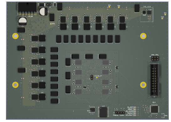
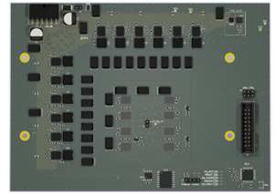
3D renders of the complete PCB (front and back)
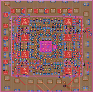
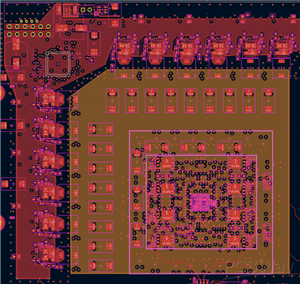
layer visualisations showing power and ground planes
close-ups of the VRM region and decoupling layout
These images highlight key layout decisions such as capacitor placement, stitching via strategy, and power routing geometry.
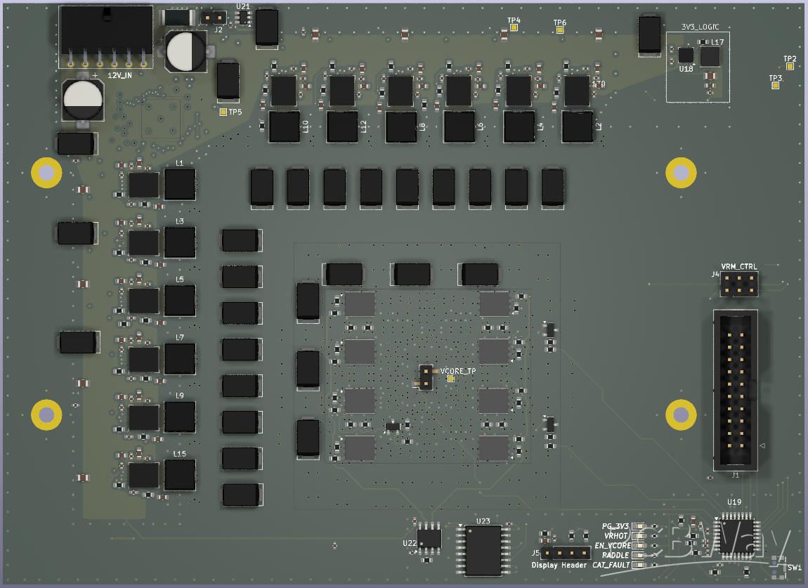
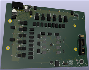
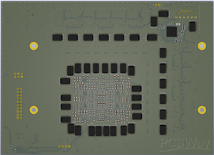
Front Side 3D Render
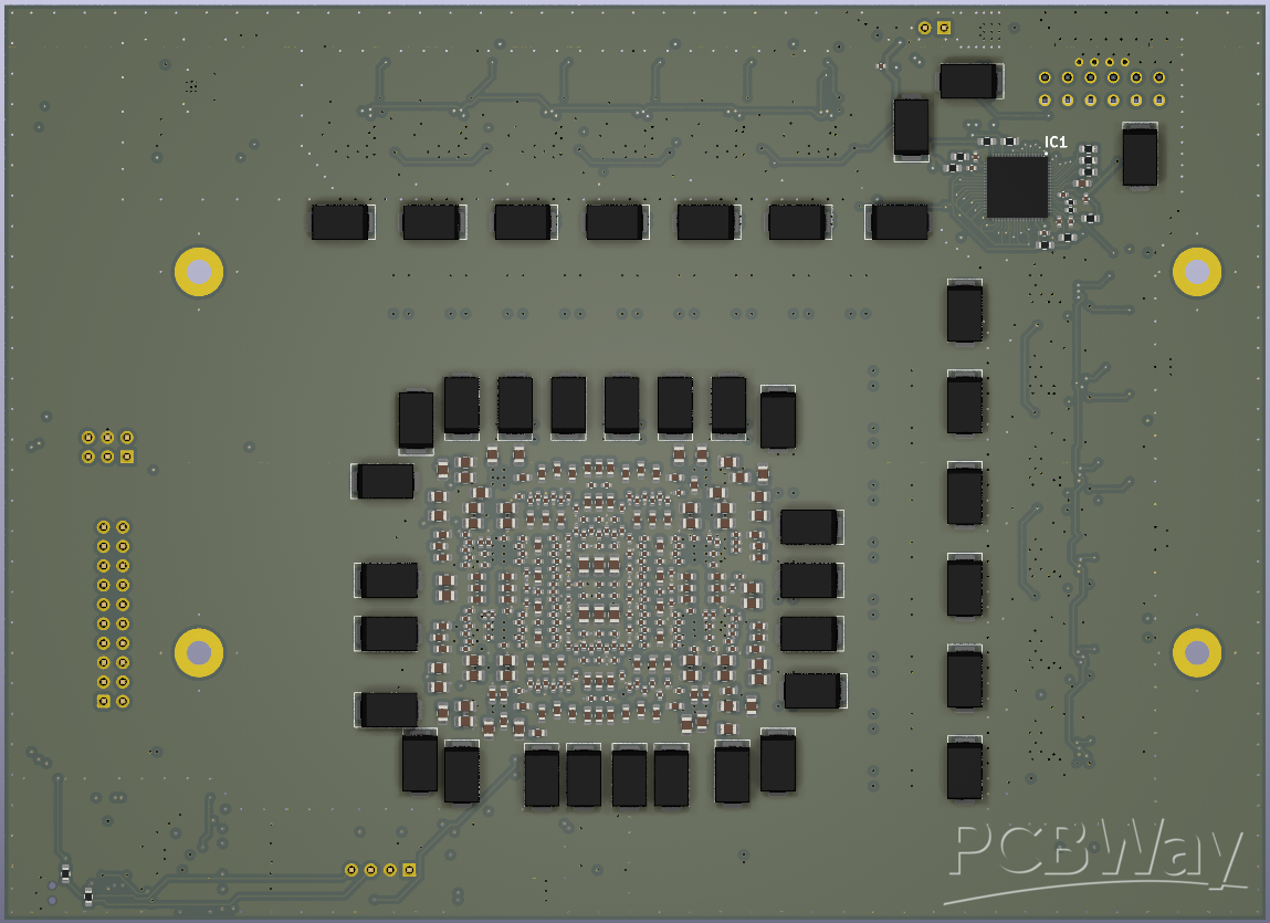
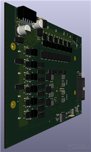
Back Side 3D Render
This project is intended not only as a design exercise, but also to be physically built and electrically tested. The board is designed to be powered from a standard ATX power supply, specifically a Corsair RM850e, using a custom jump cable to safely enable and route the 12 V rail to the board.
This approach allows the power system and load bank to be evaluated under realistic conditions using readily available hardware, while maintaining appropriate safety and control during bring-up and testing.
This project serves as both a learning platform and a professional hardware design portfolio piece, representing a complete, manufacturable power-system design from schematic through PCB layout, simulation, and planned physical validation.
Mercury Rev 1 — GPU-Class High-Current Power Delivery Test Board
*PCBWay community is a sharing platform. We are not responsible for any design issues and parameter issues (board thickness, surface finish, etc.) you choose.


Raspberry Pi 5 7 Inch Touch Screen IPS 1024x600 HD LCD HDMI-compatible Display for RPI 4B 3B+ OPI 5 AIDA64 PC Secondary Screen(Without Speaker)
BUY NOW


- Comments(2)
- Likes(1)
- 1 USER VOTES
- YOUR VOTE 0.00 0.00
-
10design
-
10usability
-
10creativity
-
10content
More by Marcus Cropley
-
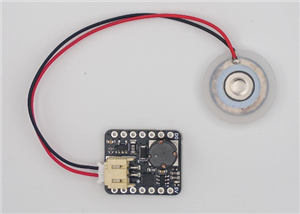
Programmable Mist Maker - XIAO / QT PY Extension
56 0 0 -
-
-
-
-
-
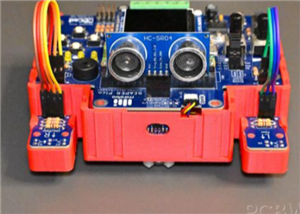
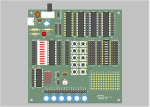
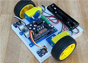
ARPS-2 – Arduino-Compatible Robot Project Shield for Arduino UNO
2708 0 5 -
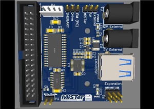
A Compact Charging Breakout Board For Waveshare ESP32-C3
3206 3 8 -
AI-driven LoRa & LLM-enabled Kiosk & Food Delivery System
3459 2 2