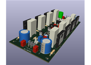


Goglotek LTD low-distortion-high-current-power-amplifier
NB: This is a free trial period project and the free trial will expire after some time and the product will be commercialized. You only pay for pcb fabrication and parts but you get a product that will rival ones costing over 2000 USD.
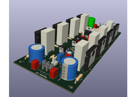
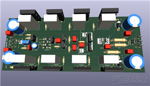
Ultra low distortion, high current, high power, high slew rate power amp boards. 1 ohm stable and low THD. It uses 4 output pairs per channel and all boards for both channels are separate for dual mono design. Untested build but the circuit simulation are solid and working perfectly. Improves on designs that have been built and used for years without issues.
Simulated amplifier results
THD 1k: 0.0000x% range at 2, 4 and 8 ohms load.
THD 20k 0.000x% range at 2, 4 and 8 ohms load.
Slew rate: at least 75 volts/microseconds
Max rail voltages:+-80v, +-100V can be achieved with >110v slim filter capacitors(only experienced builders should attempt 100v rails since any problems on the amp might damage many transistors since only the output transistors and some drivers can handle over 200V across them)
+-80V rails with 100v filter capacitors is recommended for +-70V clean power which equates to 300W into 8 ohms and more than 500W into 4 ohms
Noise: A lot of care has gone into designing the pcb and and routing traces thus it should be low. THD+N should remain in the range of the above mentioned THD.
The THD results are based transistors specified on pcb silkscreen. If you change the transistors to a different one, ensure they match or exceed the ones in the board in terms of max VCE and HFE, power and pinout(can rotate or cross legs to match). Due to the circuit being highly optimized, there is loss of headroom and max clean voltage is 10v below rail voltage. For 4 and 2 ohms speakers, it shouldn't be an issue since you will hit current limit before voltage limit. If you want more headroom for 8 ohm speakers at the cost of performance, you can remove the VAS cascode transistor on input VAS board, Q34, and solder a jumper wire between collector and emitter pads. Then replace the VAS transistor BC550, Q10, with high voltage one, e.g. 2n5551 or 2SC3503. You'll gain 5v more headroom of clean voltage each way. NB the circuit has been designed to clip cleanly and tube amp like thus on transients you won't notice clipping and transients can go up to 2V below rails without harsh transistor clipping sound. Perfect measurements can only be achieved 10v below rails and 5v below rails without cascode VAS transistor.
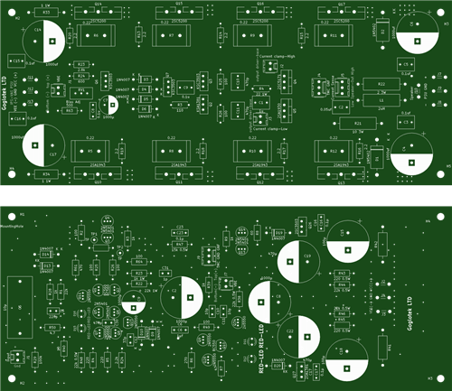
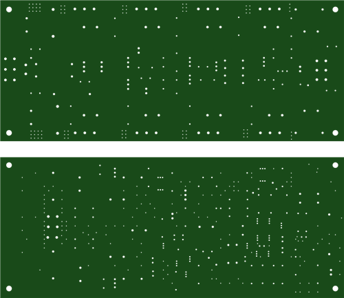
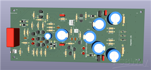
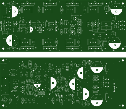
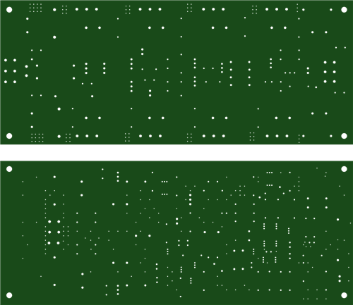
There are two boards, Input VAS board and Output board. Connections between the two boards are made using wires and connectors(can solder wires directly to pads). Mounting holes of the two boards line up perfectly thus you can stack them up, input-vas board on top of output board on heatsink. You can also mount them at 90 degrees to each other on the chassis.
Input Board:
Match input pairs transistors HFE. Transistors that are mounted facing each other should be matched and thermally coupled. Put thermal paste on their faces and squeeze them tightly. Use heat shrink tubing or zip ties to hold them together permanently. Also try to match resistors of same value close to each other at half of the board on the input side.
Output Board:
The board uses output triple configuration for high currents and low THD on high currents/low speaker impedance.
Match the 4 output pairs of transistors. The VBE multiplier transistor should be mounted on top of one of the centrally located output transistor. Solder wires to its pads and solder them to the vbe transistor. The board can handle 20 amps of current but there is a soft limiter of 15 amps. If you need more current, you can unsolder, D3, D4, D5 and D6 diodes or leave them unpopulated. There is a current sense pin which you can use to determine current flowing on one output transistor which you can multiply by 4 for total current into the speaker. The voltage between the two pins is voltage across 0.22 ohm resistor and using ohms law you can calculate current flowing through the resistor. you can divide down the voltage using resistors so that it becomes 0.6v at current limit and feed it to the base of a transistor so that it can turn it on. The transistor can open relay e.t.c. There is also a current clamp pins for use in conjunction with current sense to clamp current when it reaches a certain level to protect output transistors from over current and short circuit. To clamp current, divide down current sense voltage to be 0.6v at the set current limit level and then drive a base of shunt transistor connecting driver base pin and output pin. Connect driver base pin to collector of your shunt transistor using a diode(prevents current from flowing backwards under certain conditions) and connect the transistors emitter to output pin. There are two for both halves of the signal waveform. When pre-set current level is reached, the shunt transistor will open and steal base current from drivers which in turn will limit output base currents and thus output emitter currents gets clamped.
If you use slow pre-drivers, drivers and output transistors and encounter ringing and instability, increase values of miller capacitors c10 and c11 on Input board. You'll increase 20k THD and reduce slew rate though. Use fast transistors for pre-driver, driver and output for best performance.
Use quality genuine parts for best performance. Non-ferromagnetic resistors, connectors and capacitor leads. Filter electrolytic capacitors determine your max rail voltages thus size them appropriately with at least 10V margin for longevity. The 0.1uf capacitors should be film capacitors and the capacitors in picofarads range should be NP0, C0g through hole ceramics for best performance.
Both negative and positive feedbacks are welcome and will be used to improve the product.
Goglotek LTD low-distortion-high-current-power-amplifier
*PCBWay community is a sharing platform. We are not responsible for any design issues and parameter issues (board thickness, surface finish, etc.) you choose.


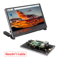
Raspberry Pi 5 7 Inch Touch Screen IPS 1024x600 HD LCD HDMI-compatible Display for RPI 4B 3B+ OPI 5 AIDA64 PC Secondary Screen(Without Speaker)
BUY NOW


- Comments(0)
- Likes(0)
 More by Engineer
-
-
ARPS-2 – Arduino-Compatible Robot Project Shield for Arduino UNO
2468 0 5 -
A Compact Charging Breakout Board For Waveshare ESP32-C3
2912 3 8 -
AI-driven LoRa & LLM-enabled Kiosk & Food Delivery System
3123 2 1 -
-
-
-
ESP32-C3 BLE Keyboard - Battery Powered with USB-C Charging
3176 0 2