
|
KiCad 9.0 |
GateLab: Logic Gate Visual Learning
Introduction
Many complex digital circuits consist of multiple logic gates each of which have one or more inputs that govern how its output responds, these gates work together to form counters, shift registers, and in turn memory, processors, and so on. Computers, mobile phones, printers and many other equipment are reliant on the circuits and components that are formed from logic gates. Thus I believe it's important that those with a passion for technology, user and designer alike, should be aware of logic gates and how they work.
Previously I had created and demonstrated a Logic function tester I had designed and built, which was a simple way to show how basic logic gates AND, NAND, OR and NOR work. Building on that, I have now created an improved version, GateLab, which demonstrates how all basic logic gates NOT (inverter), AND, NAND, OR, NOR, XOR (EX-OR), and XNOR (EX-NOR) work. However, I have only used NAND gates to create each of the aforementioned gates, which shows how it’s possible to create different logic gates using only NAND gates and has the advantage that only one type of chip is needed, the 74LS00, which contains four 2-input NAND gates.
GateLab can be run from a power bank or USB power supply and uses a number of switches (headers and jumpers in the prototype) to set the logic level for each of the gate inputs and LEDs serve as the gate outputs. This presents a fun way to learn how the basic logic gates work in an interactive manner.
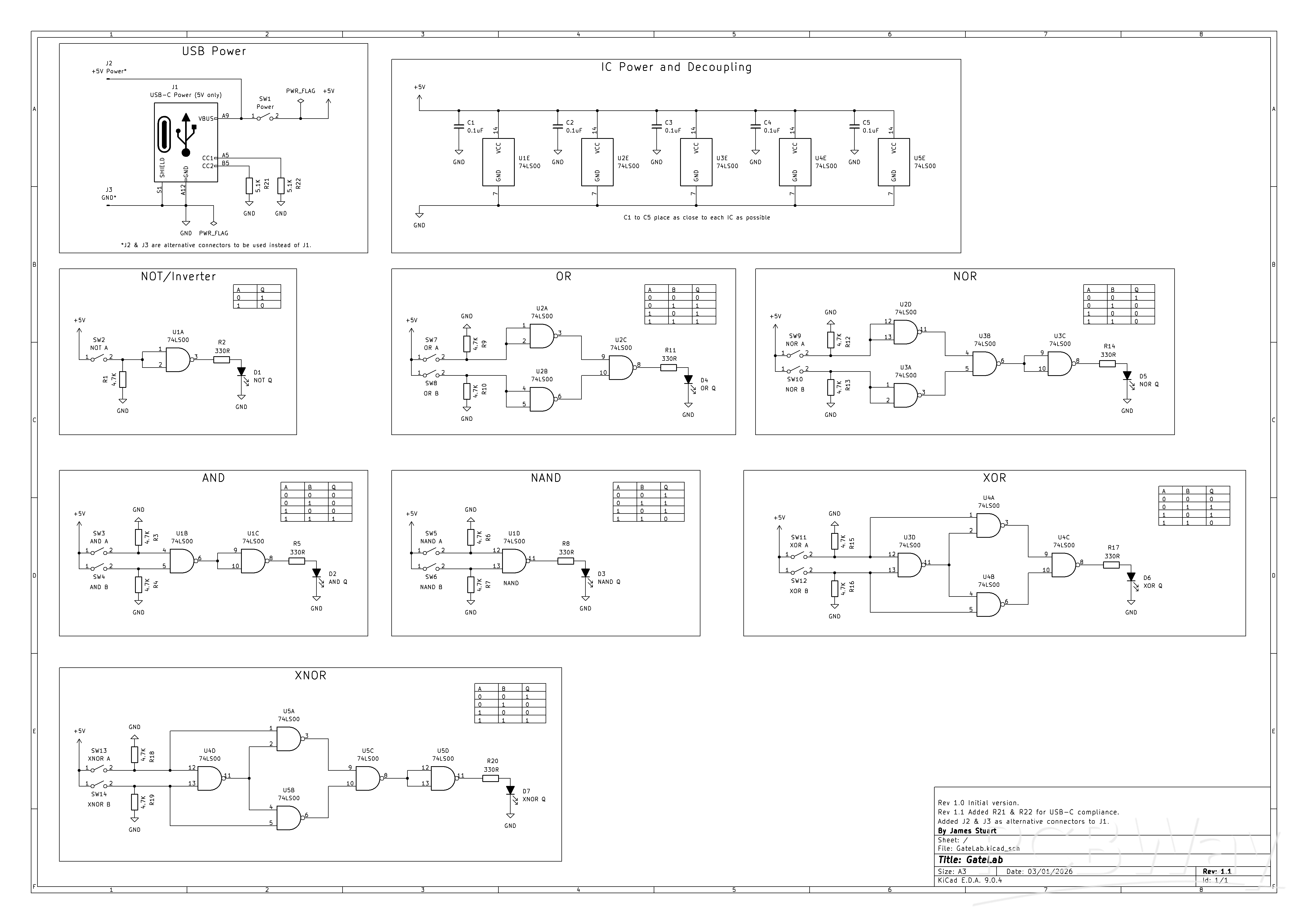
Schematic
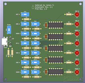
I made the schematic in KiCad 9, available below and attached to this page.

Aside from the USB connector, only through-hole components have been used, making it an approachable project for most people, even more so with rev. 1.1 of the schematic (provided on this page) which adds J2 and J3 header pins to which you can provide 5V and GND or in place of a USB connector and the header pins you can solder a USB breakout board.
J1 is the USB-C connector, providing the 5V power supply, such as provided by a phone charger, for example, which should be convenient for most people, and switch SW1 turns the power on/off. In the prototype I used a USB-C breakout board which only provides power and data (not needed) so essentially it's been used as a USB 2 connector. With schematic rev. 1.1 I added two 5.1K resistors R21 and R22 to USB-C connections CC2 and CC1 respectively to make the circuit USB-C compliant ensuring that USB-C power supplies will work. The resistors form a voltage divider with the resistors in the USB-C power source which detects the voltage and supplies power.
Each basic logic gate (NOT, AND, NAND, etc.) consists of one or more NAND gates provided by five 74LS00 ICs, U1 to U5, and truth tables for each logic gate showing the combination of input and output states are included on the schematic. You can substitute the 74LS00 for a similar, compatible version, indeed when I built the prototype I used 74AC00 ICs as I happened to have 5 of them. 74AC00 has the advantage of lower power draw compared to the 74LS00 while still providing strong output drive. Regardless of the version of 7400 you use capacitors C1 to C5, each 0.1uF, provide the power supply decoupling for the chips.
Switches SW2 to SW14 handle the inputs (A/B) to each logic gate, pulling the gate input high when in the on position. When a switch is in the off position a 4K7 resistor (R1, R3, R4, R6, R7, R9, R10, R12, R13, R15, R16, R18, R19) pulls the gate input low. Although pull-up resistors are recommended for 74LS series ICs this would result in inverted logic, since the switch would have to take the gate input low. So instead I’ve used pull-down resistors so that the input switches pull the input high when in the on position.
LEDs D1 to D7 indicate the gate output logic level. I didn't specify the LED colours on the schematic but you could use red for inverted logic gates (NOT, NAND, NOR, and EX-NOR) and green for non-inverted logic gates (AND, OR, EX-OR), for example, which will help differentiate. 330R resistors R2, R5, R8, R11, R14, R17, R20 limit the current to each LED to a moderate level. Assuming a gate output voltage of 5V (which of course in practical use it won't be but serves as the highest theoretical value) and an LED voltage drop of 2V, a 330R resistor should result in around 9mA current:
I=V/R
I=(5-2)/330
I=0.009A
This is a good compromise between battery life and LED brightness should the circuit be run off a battery. However, you should adjust the resistor value based on the LED type(s) you are using.
Prototype
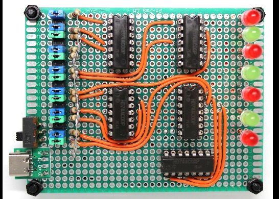
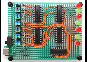
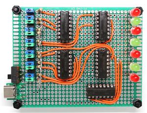
The prototype is based on schematic rev. 1.0, please see the schematic section above to learn what was added to rev. 1.1, the version attached to this page. Photos of the prototype are attached to this page and a video showing the prototype in action can be found in the Testing section.
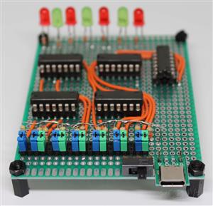
For the prototype I used components I already had and soldered them on a perfboard that has conductive isolated pads on both sides, aiming to keep the majority of wiring on the underside to keep the top side as neat as possible. Due to the limited space provided by the perfboard I had chosen and not having small enough switches, in place of switches I used a 2 x 19 male header with jumpers. This does have the advantage that the inputs can easily be driven by an external circuit. Of course you can use whichever you prefer.
Now I will go over how I soldered the circuit; I regularly checked my soldering with visual inspection and via continuity checks using a multimeter to ensure good connections where needed and that there weren't shorts were there shouldn't be. I started by soldering a USB-C breakout board to the perfboard as that would be easier than soldering a bare USB socket, then I followed with attaching the power switch.
The header was placed vertically, with the two horizontal pins removed at positions 2, 5, 8, 11, 14, and 17 to separate the inputs to the logic gates. The left side of the header pins were connected to +5V and the right side to each gate input as follows:
Header pin 1 NOT A
Header pin 3 AND A
Header pin 4 AND B
Header pin 6 NAND A
Header pin 7 NAND B
Header pin 9 OR A
Header pin OR B
Header pin NOR A
Header pin NOR B
Header pin XOR A
Header pin XOR B
Header pin XNOR A
Header pin XNOR B
Colour coded jumpers (blue for input A, green input B) were placed horizontally across the two pins to take the gate input high, or removed to cause the input to go low.
Next I soldered the LEDs with limiting resistors inline with the LED anode connections as to take up less space. After that, I soldered IC sockets (you can of course solder the chips directly to the board), due to the small size of the perfboard I put the decoupling capacitors on the board underside.
The only other thing left to do was to add any remaining wiring.
As this was the prototype I simply attached posts in the corners of the perfboard to support it on a table or other surface but you may want to put it in a project box with holes for the USB-C, switches and LEDs.
Testing
I did a number of tests between soldering the various sections; I measured the logic 1 voltage to GND of a gate to be 4.90V and the current through a red LED when the gate was on to be 8.35mA, 8.40mA for a green LED when the gate was on. This was quite close to the estimated 9mA assuming 5V gate output voltage but if we use 4.9V in the LED current formula we get 8.78mA, which better matches the readings. The red and green LEDs were both adequately bright so the chosen limiting resistors were indeed suitable.
After soldering finished and having made sure I had connected each component correctly I inserted the five chips into the sockets observing the correct orientation before connecting a phone charger for power and switching on with switch SW1. I measured 4.98V across the +5V and GND supply and measured with all LEDs off the total circuit current draw was just 9.59mA, with all LEDs on it was 62.8mA. Recall that I had used 74AC00 ICs, if you use 74LS00 chips or ICS from a different 74 family the current draw will be different. Nonetheless the circuit is suitable to be powered using batteries including running off a power bank although some power banks will switch off if the current draw is too low.
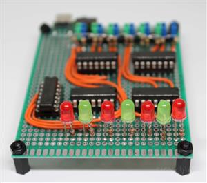
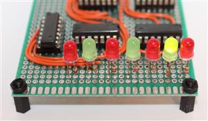
With all switches in the on position (or jumpers placed across the headers) the NOT, NAND, NOR and XOR LEDs should be off, all others on - if not, check soldering. Make sure power is getting to the circuit, in particular check the IC power pins (pins 7 and 14) and ensure the chips have been inserted/soldered the correct way round. When you have the appropriate LEDs lit go through checking that each LED lights according to the relevant truth table for each logic gate.
You can watch a demonstration of the GateLab prototype in action:
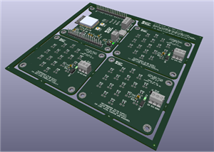
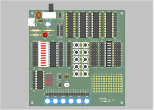
PCB
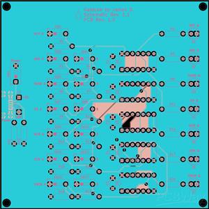
Having built and tested the prototype and found it to be working as designed I used KiCad to make the PCB layout, please note this was my first time creating a PCB design and was very much a learning process. I have attached the necessary PCB files along with 3D view and Gerber layout images.
The PCB is double sided, and measures 100 x 100mm, which should keep costs down should you have the PCB manufactured, and there are four 3mm diameter mounting holes, one in each corner, for securing to support posts, for example. Each component is labelled as necessary to indicate their reference and function, and I ensured a 5mm distance between the PCB edge and the outer components. The USB-C connector sticks out from the PCB by 2mm, which helps take off some strain from the PCB and helps make connection to a cable easier should the PCB be placed in an enclosure.
Note that although the 3D view image shows the switch arrow pointing down (power) and left (input A/B) the footprint has the 'ON' position in the opposite direction, which is the intended direction. Please check the switches you have chosen that the 'ON' position is the right way (up for power, right for input A/B.
The PCB layout has been checked for errors according to PCBWay's standards and includes the WayWayWay text on the back silkscreen layer so that the PCBWay product ID can be placed in that position should you have the PCB manufactured. However, please do let me know if you have any issues with the project including suggestions to improve it.
Conclusion
GateLab is an easy to make electronic circuit that teaches the basics of logic gates which are fundamental to many devices, the design uses cheap and easy to handle components. It shows how logic gates take one or more inputs that determne the state of its single output, and can be combined together to create other types of logic gates.
Having built the prototype and moving on to the PCB layout I improved the design by adding two pin headers for alternative power connection and the USB-C CC1 and CC2 resistors to make it USB-C compliant. Now that I've done a PCB layout I much more confident in creating more in the future.
I would like to do another version of GateLab in the future, in particular shaping the PCB to form a NAND gate, and providing the ability to easily hook up remote inputs and outputs.
GateLab: Logic Gate Visual Learning
*PCBWay community is a sharing platform. We are not responsible for any design issues and parameter issues (board thickness, surface finish, etc.) you choose.


Raspberry Pi 5 7 Inch Touch Screen IPS 1024x600 HD LCD HDMI-compatible Display for RPI 4B 3B+ OPI 5 AIDA64 PC Secondary Screen(Without Speaker)
BUY NOW


- Comments(0)
- Likes(0)
More by James Stuart
-
Programmable Mist Maker - XIAO / QT PY Extension
24 0 0 -
-
Bluetooth Speaker with Custom designed 15W dual channel Audio Amplifier
32 0 0 -
-
-
-
-
ARPS-2 – Arduino-Compatible Robot Project Shield for Arduino UNO
2700 0 5 -
A Compact Charging Breakout Board For Waveshare ESP32-C3
3192 3 8