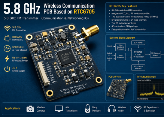
5.8 GHz Wireless Communication PCB Based on RTC6705
Project Overview
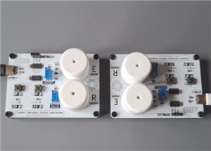
This project is a compact RF communication and networking PCB designed for experimenting with 5.8 GHz wireless transmission.
The main RF device used in this design is the RichWave RTC6705, a 5.8 GHz wide-band FM transmitter IC. The purpose of the project is to provide a practical hardware platform for studying RF signal generation, FM transmission, channel selection, RF matching, and PCB layout techniques at 5.8 GHz.
The RTC6705 integrates several important RF functions into a single IC, including a 5.8 GHz RF modulator, frequency synthesizer, VCO, PLL, audio subcarrier modulators, and power amplifier. According to the available RTC6705 documentation, the device operates from a 3.3 V supply and provides two selectable RF output power levels, with up to approximately +13 dBm referenced to the external matching network.
This makes the RTC6705 useful for compact wireless A/V transmitter designs and for engineers who want to explore practical 5.8 GHz RF PCB design.
Main Objectives
The main objectives of this project are:
- Build a practical 5.8 GHz RF transmitter PCB.
- Explore the use of the RTC6705 RF transmitter IC.
- Provide a hardware platform for RF communication experiments.
- Study 5.8 GHz PCB routing and impedance-controlled RF traces.
- Experiment with channel selection and transmitter configuration.
- Understand the importance of RF matching, grounding, shielding, and power-supply filtering.
- Provide a reusable PCB platform for wireless A/V and RF experiments.
Key Component: RTC6705
The RTC6705 is manufactured by RichWave and is designed for wide-band FM transmission in the 5.8 GHz band.
The device integrates a 5.8 GHz RF modulator with an internal VCO and PLL. It also includes two audio subcarrier modulators operating at 6 MHz and 6.5 MHz. The transmitter frequency can be configured through a three-wire SPI interface or by using dedicated digital channel-selection pins.
According to the RTC6705 datasheet, the IC supports 24 fixed-channel selections when used in the simple digital channel-selection mode. In SPI mode, the internal registers can be programmed to control the transmission frequency.
The device uses a 40-pin leadless QFN package, which keeps the RF section relatively compact but also makes PCB layout and assembly more demanding.
Important RTC6705 Features
- 5.8 GHz FM transmitter
- 3.3 V power supply
- Integrated VCO and PLL
- Integrated RF modulator
- Integrated power amplifier
- Two RF output power levels
- SPI-based frequency programming
- Digital fixed-channel selection
- 6 MHz and 6.5 MHz audio subcarrier modulators
- 40-pin leadless QFN package
- Designed for wireless A/V transmission applications
Hardware Architecture
The PCB can be divided into several functional sections:
1. RF Transmitter Section
The RTC6705 is the core of the RF transmitter.
The RF section contains the required external components around the RTC6705, including the RF matching network and associated filtering components. Because the operating frequency is around 5.8 GHz, the physical PCB layout becomes part of the RF circuit.
Short RF traces, controlled impedance, a continuous ground reference, and appropriate component placement are important for maintaining predictable RF performance.
2. Control Interface
The RTC6705 supports a three-wire SPI interface for transmitter configuration.
The control interface can be connected to an external microcontroller or another digital controller. The controller can be used to configure the desired transmission channel and other programmable functions.
For applications that do not require an external MCU, the RTC6705 also provides a simple digital channel-selection mode using dedicated pins. This allows predefined channels to be selected directly by hardware.
3. Power Supply
The RTC6705 is specified for a 3.3 V supply.
The PCB should provide appropriate power filtering close to the IC. Separate attention should be given to the digital, analog, PLL/VCO, and RF power paths where applicable.
For RF designs, a clean supply is important because supply noise can couple into sensitive oscillator and RF circuits.
4. RF Output and Antenna Interface
The RF output should be routed through the appropriate matching network before reaching the antenna connector or antenna structure.
At 5.8 GHz, even a short PCB trace can have a significant electrical effect. Component placement, trace width, ground-via arrangement, connector selection, and PCB stack-up should therefore be considered together rather than independently.
PCB Layout Considerations
One of the main purposes of this project is to demonstrate that a 5.8 GHz design requires a different PCB layout approach from a low-frequency digital board.
Keep RF Connections Short
The RF path between the RTC6705, matching components, and antenna interface should be kept as short as practical.
Unnecessary bends, vias, long traces, and unused copper around the RF path should be avoided unless they are part of the intended RF design.
Use a Solid Ground Reference
A continuous ground plane provides a low-impedance return path and helps reduce unwanted RF coupling.
Ground vias can also be placed around sensitive RF sections where appropriate. However, via placement should follow the actual RF layout requirements rather than simply adding vias everywhere.
Place Matching Components Close to the RF Pin
The RF matching network should be positioned close to the relevant RF output.
The distance between the IC and matching components directly affects the RF characteristics of the interconnect. At 5.8 GHz, the PCB trace is no longer electrically negligible.
Separate Digital and RF Areas
The digital control signals should be routed so that unnecessary coupling into the RF section is minimized.
The SPI lines should not be routed through the most sensitive RF area unless the layout requires it.
How the Project Works
A typical operating sequence is:
- Apply the required 3.3 V supply.
- Initialize the RTC6705.
- Configure the desired transmission channel.
- Provide the required baseband/video and audio signals.
- The RTC6705 modulates the input information onto the RF carrier.
- The internal RF circuitry generates the 5.8 GHz transmission signal.
- The integrated power amplifier provides the RF output.
- The external matching network transfers the RF signal to the antenna.
The RTC6705 supports both SPI programming and hardware channel selection, giving the PCB flexibility for different control architectures.
Possible Applications
The RTC6705 documentation lists applications such as A/V transmitters, wireless cameras, baby monitors, wireless audio equipment, and wireless earphones.
A PCB based on this architecture can therefore be useful for:
- 5.8 GHz RF experiments
- Wireless camera experiments
- Analog A/V transmission
- Wireless audio experiments
- RF transmitter development
- RF PCB layout learning
- Channel-selection experiments
- Embedded RF development
- Prototype wireless communication systems
The actual operating frequency, transmission power, antenna configuration, and legal use of the finished product must comply with the applicable radio regulations in the target country or region.
Why Use RTC6705 in This Project?
A major advantage of the RTC6705 is its level of integration.
Instead of implementing the RF oscillator, PLL, VCO, modulator, and power amplifier as separate functional blocks, the RTC6705 integrates these functions into one RF IC. This can reduce the number of active RF devices and make the overall transmitter architecture more compact.
For PCB designers, however, high integration does not eliminate RF design challenges. The matching network, PCB stack-up, grounding, supply decoupling, RF trace geometry, shielding, and antenna interface still need to be designed carefully.
This makes the project particularly useful as a practical example of the relationship between an RF IC and its PCB layout.
Testing and Debugging
When bringing up the board, I recommend checking the system in stages rather than connecting everything at once.
First, verify the 3.3 V supply and confirm that the power rails remain stable during startup.
Next, check the digital control interface and confirm that the RTC6705 receives the expected configuration data.
After that, verify the RF output using suitable 5.8 GHz test equipment, such as a spectrum analyzer and appropriate RF measurement accessories.
For RF measurements, the test setup itself can affect the result. The cable, connector, matching network, antenna, and measurement instrument should therefore be considered part of the complete RF system.
If the RF output is lower than expected, possible areas to investigate include:
- Incorrect matching-network values
- PCB stack-up differences
- RF trace geometry
- Poor grounding
- Power-supply noise
- Incorrect channel configuration
- Connector or cable losses
- Antenna mismatch
- Component placement
What I Learned From This Design
The most important lesson from this project is that a 5.8 GHz PCB cannot be treated simply as a conventional digital PCB.
At lower frequencies, a small change in trace length may have little practical impact. At 5.8 GHz, the same trace can become an important part of the RF circuit.
The RTC6705 provides a highly integrated RF transmitter solution, but the PCB still determines how effectively the IC can be connected to the outside world.
For this reason, the RF section should be designed together with the PCB stack-up, impedance requirements, matching network, grounding strategy, and antenna interface from the beginning of the project.
Project Files
The following files can be included with this PCBWay project:
- Schematic
- PCB layout
- Gerber files
- BOM
- Pick-and-place/Centroid file, if available
- 3D PCB model, if available
- Assembly drawings
- Test notes
- Firmware or configuration code, if applicable
Please make sure that the uploaded files correspond to the actual PCB revision shown in the project images.
Conclusion
This project provides a practical 5.8 GHz wireless communication PCB centered around the RichWave RTC6705.
The project combines an integrated RF transmitter IC with a carefully designed PCB RF section, digital control interface, power supply, matching network, and antenna interface.
Beyond the transmitter itself, the project is intended to provide a useful example of 5.8 GHz PCB design, including RF routing, grounding, impedance control, power filtering, and RF debugging.
For engineers and makers working with wireless communication hardware, the RTC6705 provides an interesting example of how a highly integrated RF IC can simplify the active circuitry while still requiring careful PCB-level RF engineering.
5.8 GHz Wireless Communication PCB Based on RTC6705


Raspberry Pi 5 7 Inch Touch Screen IPS 1024x600 HD LCD HDMI-compatible Display for RPI 4B 3B+ OPI 5 AIDA64 PC Secondary Screen(Without Speaker)
BUY NOW

- Comments(1)
- Likes(1)
More by Avaq Semiconductor

-
Émetteur Récepteur Optique Expérimental (communication UART ATtiny + fibre optique)
25 0 1 -
SmallOLED - Live PC Stats, Animated Clocks & Audio Visualizer
861 0 3 -
"Talking Multimeter": Arduino-Based Speech Add-on for Multimeters with SCPI Protocol
505 0 1 -
Programmable Mist Maker - XIAO / QT PY Extension
2973 2 3 -
RadioHAT - Raspberry Pi radio development platform
2519 0 4 -
-
-