What Is Solder Joint Inspection?
In the PCB industry, solder joint inspection is the process of checking whether the solder connections between electronic components and the printed circuit board (PCB) are strong, reliable, and free from defects. These solder joints provide both the electrical connection and the mechanical support that allow a circuit to work correctly. If a solder joint fails, the entire product may stop working, even if all the components themselves are perfectly good.
Think of solder joints as the "glue and wiring" of a PCB. Every resistor, capacitor, microcontroller, connector, and integrated circuit depends on good solder joints to function properly. A poor solder joint can cause intermittent failures, overheating, short circuits, or complete product failure.
Why Is Solder Joint Inspection Important?
As an electronics engineer, I often tell beginners that most PCB failures are not caused by bad components. They are caused by manufacturing issues, and soldering defects are among the most common.
A good solder joint should:
- Create a solid electrical connection
- Provide mechanical strength
- Resist vibration and temperature changes
- Remain reliable throughout the product's life
Without proper inspection, hidden defects can reach customers and lead to expensive repairs, warranty claims, or safety risks. This is why professional PCB manufacturers spend significant time inspecting solder joints during production.
What Does a Good Solder Joint Look Like?
A properly formed solder joint usually has:
- Good wetting between the component lead and PCB pad
- A smooth appearance
- A clean fillet shape
- No cracks or gaps
- No unintended connections to nearby pads
According to industry inspection standards, inspectors look for clear evidence that the solder has bonded correctly to both surfaces.
Common Solder Joint Defects
During inspection, engineers search for defects that could reduce reliability.
1. Cold Solder Joint
A cold solder joint occurs when the solder does not melt or flow properly during soldering.
Signs include:
- Dull appearance
- Rough surface
- Weak electrical connection
These joints may work initially but often fail later.
2. Solder Bridge
A solder bridge happens when solder accidentally connects two conductors that should remain separate.
Problems caused:
- Short circuits
- Device malfunction
- Potential board damage
Solder bridges are among the most common defects found during inspection.
3. Insufficient Solder
Too little solder can create weak mechanical and electrical connections.
Possible results:
- Intermittent operation
- Open circuits
- Reduced durability
4. Excess Solder
Too much solder may hide defects or create stress on the joint.
Although the board may still function, excessive solder is often considered a process quality issue.
5. Cracks
Cracks may develop due to:
- Mechanical vibration
- Thermal cycling
- Improper manufacturing
Even tiny cracks can eventually cause failure.
6. Voids
Voids are small air pockets trapped inside the solder.
Large voids can:
- Reduce mechanical strength
- Increase heat buildup
- Lower reliability
Many voids cannot be seen from the outside and require X-ray inspection.
Methods Used for Solder Joint Inspection
Modern PCB manufacturing uses several inspection methods. Each has advantages and limitations.
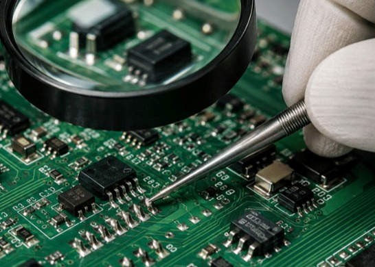
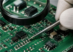
1. Visual Inspection
Visual inspection is the simplest method.
Inspectors use:
- Good lighting
- Magnifying lenses
- Microscopes
They check for obvious defects such as:
- Bridges
- Missing solder
- Misaligned components
- Poor wetting
Visual inspection is fast and inexpensive but cannot detect hidden defects.
2. Manual Optical Inspection (MOI)
Manual Optical Inspection is a more detailed version of visual inspection.
Technicians carefully examine solder joints under magnification and compare them against quality standards.
Advantages:
- Low cost
- Flexible
- Good for prototypes
Disadvantages:
- Depends on operator skill
- Slower than automated systems
- May miss small defects
3. Automated Optical Inspection (AOI)
AOI is one of the most widely used inspection methods in PCB assembly.
AOI machines use:
- High-resolution cameras
- Image processing software
- Automated defect detection
The system compares actual PCB images with reference data and identifies problems automatically.
AOI can detect:
- Solder bridges
- Missing components
- Incorrect component orientation
- Insufficient solder
Because AOI is fast and consistent, it is commonly used in mass production.
4. X-Ray Inspection (AXI)
Some solder joints are hidden beneath components such as:
- BGA packages
- QFN packages
- Advanced ICs
Traditional cameras cannot see these joints.
X-Ray Inspection (AXI) allows engineers to examine the inside of the assembly without damaging it.
X-ray systems can detect:
- Voids
- Hidden bridges
- Cracked joints
- Insufficient solder
- Head-in-pillow defects
For modern high-density PCBs, X-ray inspection is often essential.
5. Electrical Testing
Inspection alone does not guarantee that a board functions correctly.
Manufacturers often perform:
- In-Circuit Testing (ICT)
- Functional Testing (FCT)
These tests verify that electrical connections work as intended after soldering.
Industry Standards for Solder Joint Inspection
Professional PCB manufacturers generally follow industry standards when inspecting solder joints.
The most widely used standard is:
- IPC IPC-A-610
This standard defines what is:
- Acceptable
- A process indicator
- A defect
It provides detailed visual examples and acceptance criteria for different product reliability levels. Many inspectors and quality engineers are trained specifically on IPC-A-610 requirements.
Challenges in Modern PCB Inspection
PCB technology continues to become smaller and more complex.
Today's boards often include:
- Fine-pitch components
- BGAs
- HDI designs
- Miniaturized packages
Many critical solder joints are completely hidden from view. As a result, manufacturers increasingly combine multiple inspection methods such as:
- Solder Paste Inspection (SPI)
- AOI
- X-Ray Inspection
- Electrical Testing
This layered approach helps catch defects before products reach customers.
The Future of Solder Joint Inspection
The industry is increasingly using Artificial Intelligence (AI) and machine learning to improve inspection accuracy.
Modern systems can analyze thousands of solder joints in seconds and automatically identify defects that might be missed by human inspectors. Research shows that AI-assisted inspection can improve consistency while reducing manual workload.
Conclusion
Solder joint inspection is one of the most important quality-control steps in PCB manufacturing. Its purpose is to ensure that every solder connection is electrically sound, mechanically strong, and reliable throughout the product's life.
Engineers use visual inspection, AOI, X-ray inspection, and electrical testing to identify defects such as solder bridges, cold joints, cracks, insufficient solder, and voids. By following standards such as IPC-A-610 and using modern inspection technologies, manufacturers can significantly improve PCB reliability and reduce field failures.
In simple terms, if soldering builds the connection, solder joint inspection is what ensures that connection can be trusted.
What Is Solder Joint Inspection?

- ✖ | No sharing or redistributing in any way of the 3D files or derivatives
- ✖ | No remixing
- ✖ | Non-commercial Use (only for personal use)


Raspberry Pi 5 7 Inch Touch Screen IPS 1024x600 HD LCD HDMI-compatible Display for RPI 4B 3B+ OPI 5 AIDA64 PC Secondary Screen(Without Speaker)
BUY NOW

- Comments(1)
- Likes(1)
More by Avaq Semiconductor
-
Programmable Mist Maker - XIAO / QT PY Extension
1055 2 1 -
RadioHAT - Raspberry Pi radio development platform
853 0 2 -
-
-
-
-
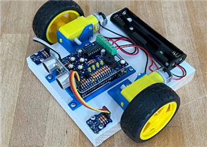
ARPS-2 – Arduino-Compatible Robot Project Shield for Arduino UNO
3317 0 6 -
A Compact Charging Breakout Board For Waveshare ESP32-C3
3922 3 8 -
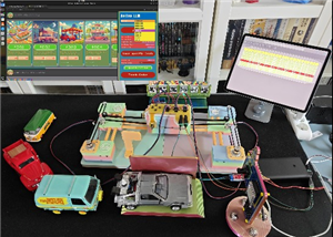
AI-driven LoRa & LLM-enabled Kiosk & Food Delivery System
4310 2 2