
|
KiCADKicad
|
BenchIO: Your Prototyping Sidekick
Introduction
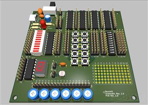
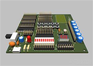
When I’m prototyping, testing and debugging circuits I often need various components, including switches, LEDs, resistors, and so on. This project, BenchIO, combines commonly needed components on a small 10 x 10 cm PCB, which is easy to carry around and cheap to manufacture. Headers provide connections to the onboard components and there are multiple power headers for additional convenience. Although BenchIO is geared toward digital electronics it can be used for general purpose.
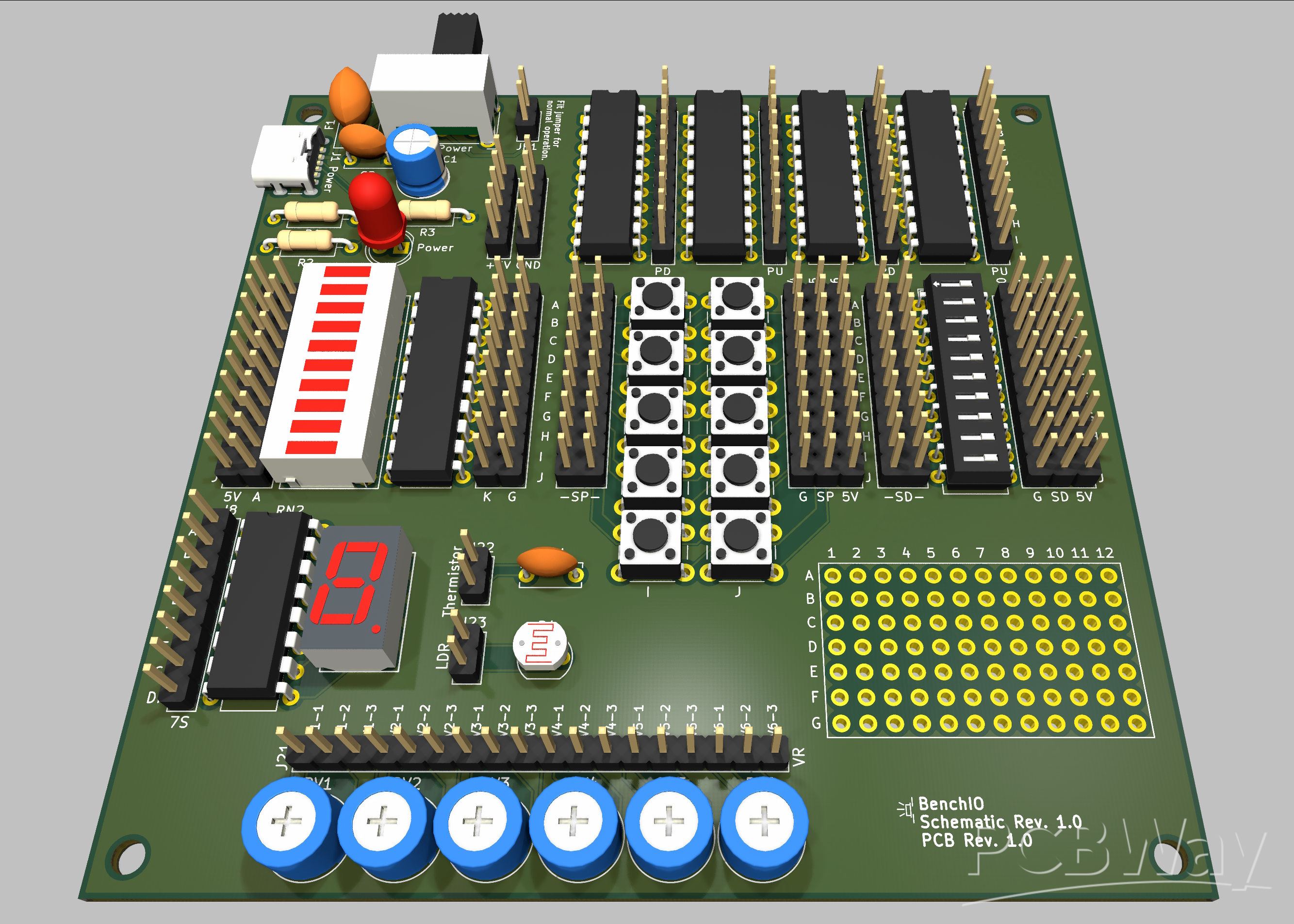
The features are as follows:
Powered by USB-C
Resettable fuse protection
Inline current measurement points
General purpose power pins
10 LED bargraph display
7-segment LED display
10 switches in DIP package
10 push buttons
20 pull-up and 20 pull-down resistors
6 potentiometers
Thermistor
LDR
12 x 7 prototyping soldering area
All of the components that make up BenchIO, apart from the USB-C connector, are through-hole, making it straightforward to be soldered by most people.
Schematic
I created the schematic using KiCad 10, please refer to it as I explain how the BenchIO circuit works.
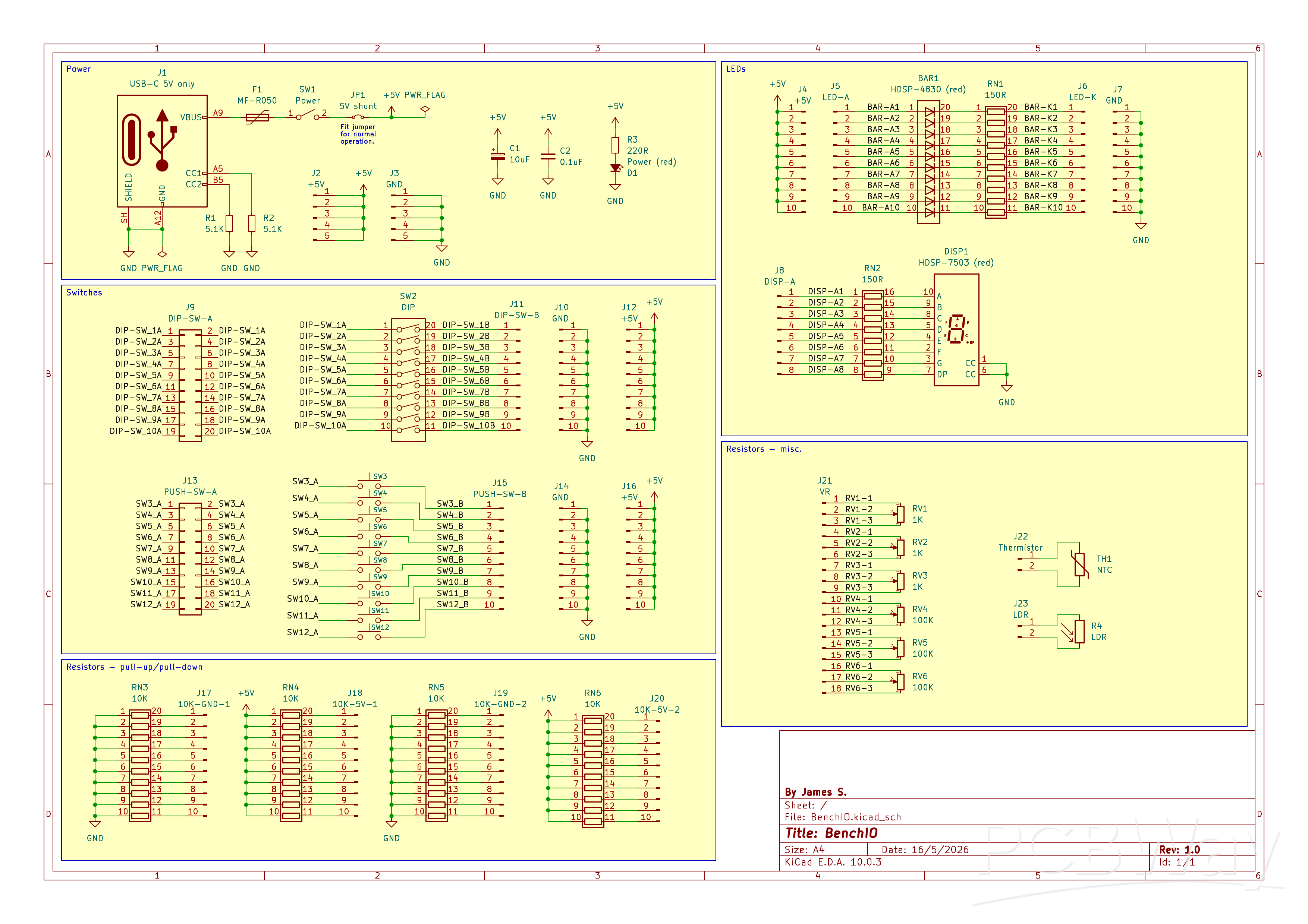 To power BenchIO, connect a 5 VDC 0.5 A maximum power supply to USB-C connector J1, 0.5 A should be more than enough for all the onboard components (<400 mA) as well as providing some power for additional components. USB-C was chosen as USB-C power supplies are very common and provide regulated 5V with the convenience of a reversible connector.
Note that a computer USB port will likely limit current draw to 100 mA so it is recommended to use a USB power supply connected to the mains rather than a computer USB socket if you need more than 100 mA.
To ensure compatibility with all USB-C power supplies (or at least those that adhere to the USB-C specification), two resistors, R1 and R2 (both 5.1 K) ground the USB-C CC1 and CC2 pins, signalling to the USB-C power supply to deliver 5V, acting as enable signals.
Due to the nature of BenchIO there is likelihood of shorts and while typical USB-C power supplies will have current limiting I have included a polyfuse (F1), type MF-R050, which has a hold current of 0.5 A and trip current of 1 A, guaranteeing that at least 0.5 A will be handled without tripping the fuse.
Switch SW1 turns power on and off and JP1 is a male 2-way header with a jumper across it that enables 5 V for normal operation but the jumper can be removed and an ammeter (or multimeter in A/mA mode) can be connected to measure current draw while BenchIO is powered.
C1 and C2 provide bulk decoupling and help with noisy USB power supplies and LED D1 indicates that power is available, the LED is current limited via resistor R3 (220R), to give ~13 mA.
Headers J2 (+5V) and J3 (GND) provide power to external circuits and can also be used as test points.
Moving on to the outputs, starting with BAR1, which is a 10 LED bar graph display, all red LEDs, type HDSP-4830, which is rated for 30mA per LED but I have chosen the limiting resistors, provided by resistor array RN1, to be 150 R for 20 mA to help extend the LED life. Change the LED array for another type with the same pinout or use individual LEDs if preferable and adjust RN1 if necessary. Note that individual resistors could be used instead of a resistor array.
The anodes of BAR1 are available on header J5 and jumpers can be placed across J5 and header J4, which carries +5V, if you need to tie the anodes high. Header J6 carries BAR1 cathodes and jumper J7 is connected to GND so in a similar manner jumpers can be placed across J6 and J7 to connect the cathodes to GND if required.
The other form of output is a HDSP-7503 7-segment red common cathode LED display with d.p. (DISP1) rated for 30 mA per LED and as with the bar graph display, resistor array RN2 was chosen for 20 mA per LED to help extend the LED life. The display anodes are on header J8 and of course the common cathode pins are connected to GND.
There are a number of different inputs including two lots of switches, the first of which are 10 switches contained in a DIP package, SW2. One side of the switches (side A) are connected to a 2 x 10 header J9, which has the switch side A connections duplicated, so that you can connect to an external circuit (e.g. a MCU) and pull-up or pull-down resistors such as provided by BenchIO (more on that later).
Switches side B are connected to header J11, and headers J10 and J12 carry GND and +5V respectively so that you can tie the switches to GND or +5V by placing jumpers either across J10 and J11 or J10 and J12.
The second type of switches are the push buttons, SW3 to SW12, which are accessible by 2x10 header J13 for side A, such that they can be connected to an external circuit and pull-up or pull-down resistors. Side B of the switches are connected to header J15, and headers J14 and J16 provide connections to GND and +5V respectively.
Four resistor arrays (RN3 to RN6), all 10K, are commoned one side to either GND (RN3 and RN5) or +5V (RN4 and RN6), intended to be used as pull-down/pull-up resistors for the onboard switches or for an external circuit. Headers J17 to J20 provide the connections to the resistors.
Next we have six potentiometers, RV1 to RV6 are, RV1 to RV3 are 1K, and RV4 to RV6 are 100K, both are common values but of course you can fit other values should you wish to. Regardless of the values used, it is intended that the trimmer type is used, preferably the type that can be adjusted with a screwdriver or by hand. Header J21 provides connections to the potentiometers.
Lastly, we have an NTC thermistor, TH1, accessible through header J22, and an LDR (light-dependent resistor), via header J23. Substitute these components with different types as required.
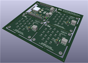
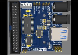
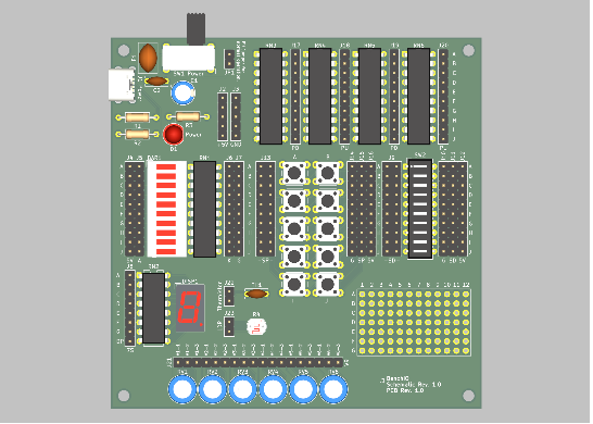
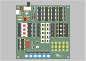
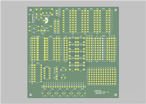
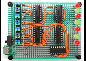
PCB
I designed the PCB in KiCad based on the schematic, please take a look at the 3D renders of the PCB that I have provided.

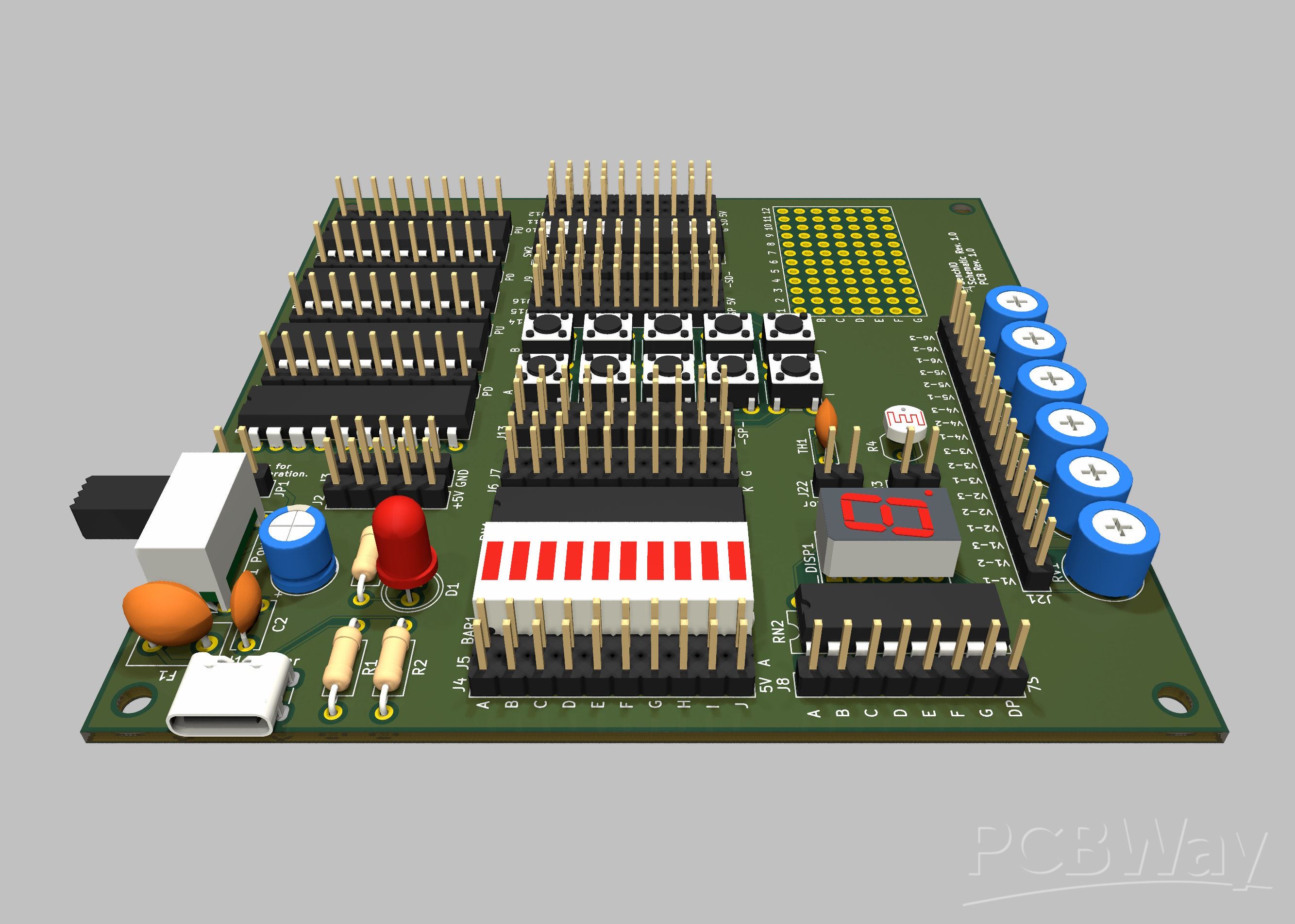
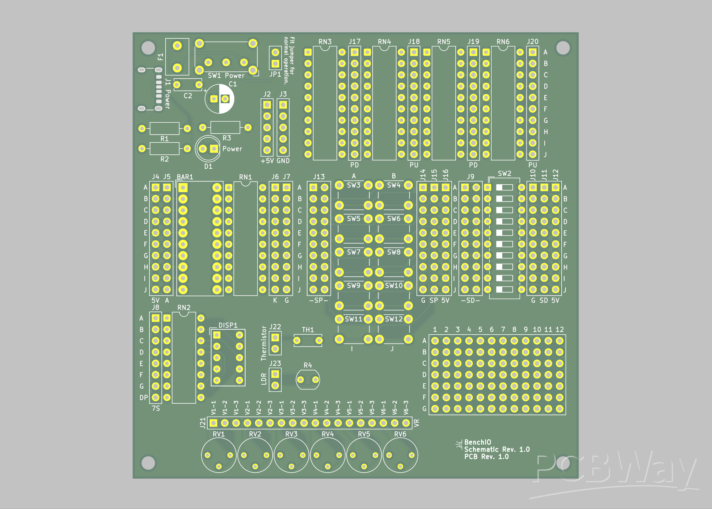
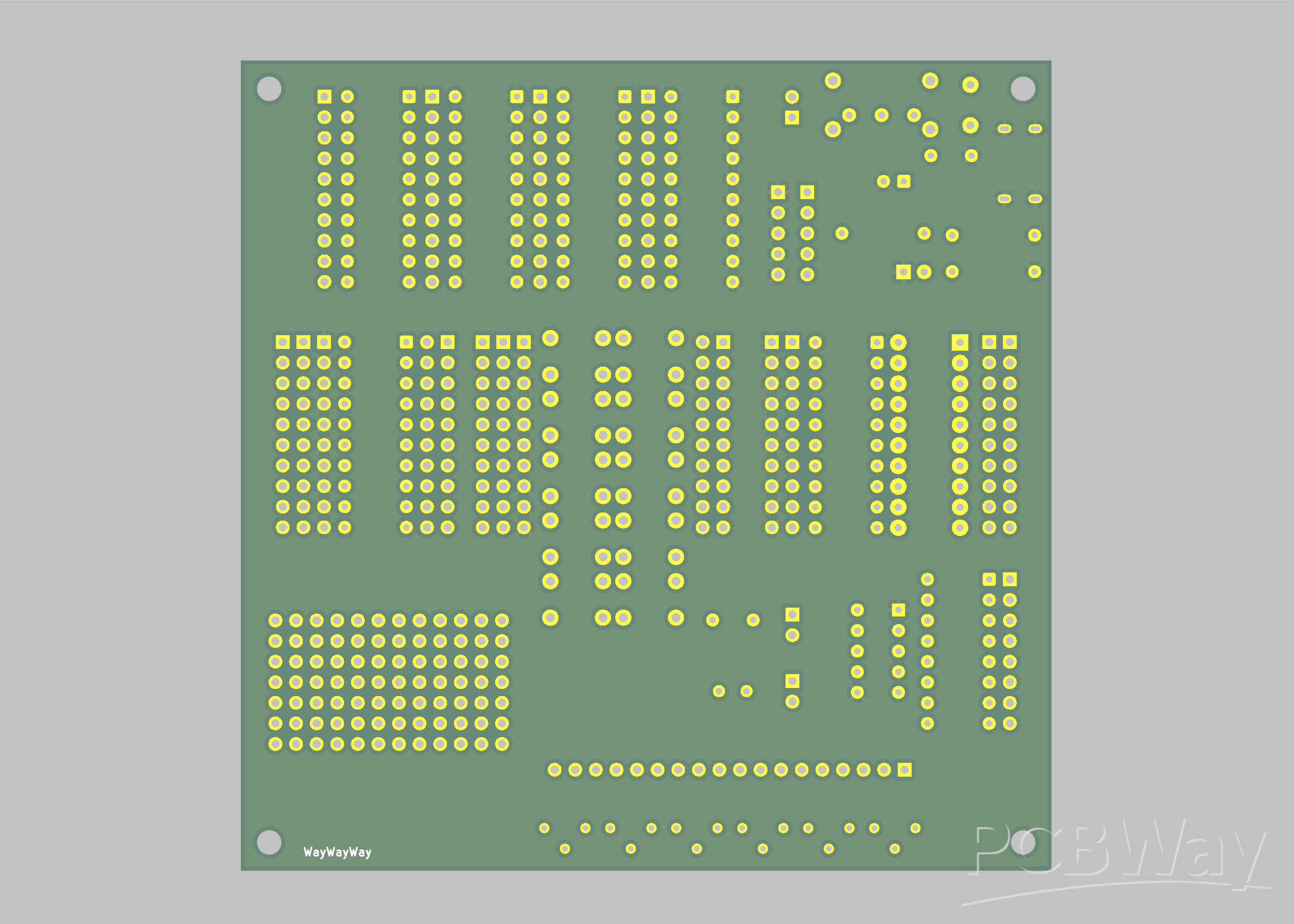
The PCB layout has been checked for errors according to PCBWay's standards and includes the WayWayWay text on the back silkscreen layer so that the PCBWay product ID can be placed in that position should you have the PCB manufactured.
BenchIO uses a single 10 x 10 cm double-sided PCB, featuring four 3 mm diameter mounting holes, one in each corner. The PCB has a +5V plane on the top side, and a GND plane on the bottom side, which greatly simplified the routing process and allowed for traces on the top side only, resulting in a neater look. The other advantages of using the planes is to keep consistent voltage levels and to help distribute current throughout the circuit.
The USB-C socket (J1) sticks out slightly from the PCB to help relieve stress from the PCB when inserting or removing a cable and to help with fitting in an enclosure should that be desired. I chose a USB-C footprint that has through-hole shield pins while the power and CC1 and CC2 connections are surface mount. If soldering the PCB by hand it may be desirable for the USB-C connector shield pins to stick out from the bottom of the PCB to make soldering them easier, in which case I would recommend having the PCB manufactured with a thickness of 0.8 mm rather than the more common 1.6 mm.
All the headers have been labelled but due to lack of room I have abbreviated some of the labels:
7S = 7-segment
A = anode
G = GND
K = cathode
LDR = light-dependent resistor
PD = pull-down
PU = pull-up
SD = Switch DIP
SP = switch push button
VR = variable resistor (potentiometer)
The switches (SW2 to SW12) were placed underneath the resistor arrays (RN3 to RN6) to minimize the length of wires needed to connect them together but all components should be reachable with standard length jumper wire.
I added a 'breadboard' prototype area to the PCB, which is not part of the schematic, consisting of a matrix of 12 x 7 standard size holes (1 mm) spaced 2.54 mm apart in both directions, in which you can solder whatever components you need to. The prototype area was created by adding to the PCB seven 12 pin header footprints spaced out vertically with a distance of 2.54 mm. For each header I hid the 3D model so it didn’t show in the 3D Viewer.
Since the PCB is designed to handle up to 0.5A we need to consider the PCB trace width. While the default 0.2 mm trace width should be able to handle 0.5 A (assuming trace thickness of 25 um), I increased the traces involving the power section (J1, F1, SW1 and JP1) to 0.5 mm, which should allow for at least 1 A.
For the thermistor (TH1) and polyfuse (F1) I used a disc capacitor footprint as I couldn’t find a suitable footprint in Kicad but a disc capacitor closely resembles those components. Similarly, for the resistor array footprint I used an IC-like DIP package footprint, which is appropriate for DIP resistor arrays.
Testing
A suitable power supply should be connected to the USB-C socket (J1), the power switch (SW1) moved to the on position, and a jumper should be placed across JP1 unless the current draw is to be measured, in which case an ammeter should be connected with the + (positive) lead on JP1 bottom pin and the - (negative) lead on JP1 top pin. LED D1 should be illuminated and power should be available across J2 (+5V) and J3 (GND). If not, double check all soldered connections in the power section, checking for continuity between traces and components, and ensure D1 has been soldered with the correct polarity.
If D1 is illuminated and power is available on J2 and J3 you can move on to testing the other components, such as the LEDs. For example, to test the bar graph LED display (BAR1) you can place jumpers across J4 and J5 to connect the anodes to +5V and jumpers across J6 and J7 to connect the cathodes to GND, causing the LEDs to light.
The switches could be tested by putting them in series with the bar graph display, for example to test the DIP switch (SW2) place jumpers across J10 and J11 to connect one side of the switch to GND. Then run wires from either side of J9 to J6 to connect the switches to the bar graph display and place jumpers across J4 and J5 to connect the anodes to +5V. Putting the DIP switches into the on positions will light the corresponding LED on the bar graph display.
For testing the potentiometers (RV1 to RV6), resistor arrays (RN3 to RN6), thermistor (TH1), and LDR (R4), probably the easiest way is with a ohmmeter or multimeter in resistance mode while BenchIO isn’t powered.
Conclusion
BenchIO provides a convenient assortment of components on a PCB in a small form factor, ideal for developing, prototyping and testing a wide range of circuits. It features mostly through-hole, readily available components that are easy to handle and straightforward to solder. It is suitable for beginners and advanced users and should prove useful to a hobbyist and repair person alike.
I welcome feedback on the project including how the design could be improved.

BenchIO: Your Prototyping Sidekick
Project images are for reference only. Actual production is based on the manufacturing files on the project page.
Please review the designer's notes (e.g., PCB thickness) and select the appropriate options.
PCBWay is not responsible
for issues caused by unsuitable parameter selections.
For more important ordering information, please refer to
Read More


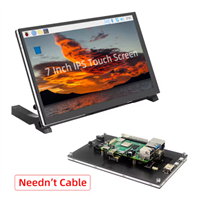
Raspberry Pi 5 7 Inch Touch Screen IPS 1024x600 HD LCD HDMI-compatible Display for RPI 4B 3B+ OPI 5 AIDA64 PC Secondary Screen(Without Speaker)
BUY NOW


- Comments(1)
- Likes(3)
More by James Stuart
-
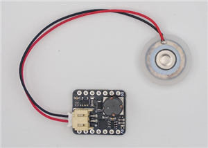
Programmable Mist Maker - XIAO / QT PY Extension
1014 2 1 -
RadioHAT - Raspberry Pi radio development platform
816 0 2 -
-
-
-
-
ARPS-2 – Arduino-Compatible Robot Project Shield for Arduino UNO
3276 0 6 -
A Compact Charging Breakout Board For Waveshare ESP32-C3
3895 3 8 -
AI-driven LoRa & LLM-enabled Kiosk & Food Delivery System
4276 2 2