Sound mixed signal pcb design requires a fundamental understanding of both analog and digital circuits to minimize, if not fully prevent, signal interference. Modern electronic systems integrate components operating in both the digital and analog domains, and careful design is essential to preserve signal integrity across the entire system.
As a critical phase of mixed-signal system development, PCB layout can be challenging, and component placement is only the first step. Additional factors must be taken into account, including board stackup and proper layer management, to reduce interference caused by parasitic capacitance that may form unintentionally between PCB planes.
Grounding is another essential element of well-executed mixed signal pcb layout. While grounding remains a widely debated topic in the industry, establishing a standardized methodology is rarely straightforward for engineers. Even a single issue with high-quality grounding can compromise the entire layout of a high-performance mixed-signal board, making this aspect too important to overlook.
Before placing circuit components, a system floorplan must be created. This step lays the foundation for overall design integrity and helps avoid interference from high-noise signals.
When developing the floorplan, it is recommended to follow the signal paths defined in the schematic, especially for high-speed circuits. Component positioning is also a key design consideration. Designers should identify critical functional blocks, signal paths, and interconnections between modules to determine the optimal location for each component. For instance, connectors are best placed along the board edge, while supporting components such as decoupling capacitors and crystals must be positioned as close as possible to mixed-signal devices. These placement rules align with basic mixed signal pcb design guidelines for floorplanning.
To minimize shared return paths for analog and digital signals, separating analog and digital blocks is a core practice for designing a high-performance mixed signal pcb, preventing digital noise from contaminating analog signals.
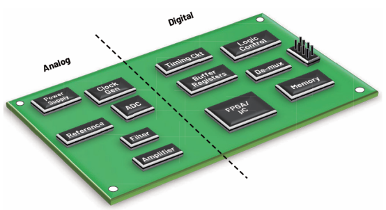
(Figure 1: illustrates a good example of analog and digital circuit separation)
When partitioning analog and digital sections, the following considerations apply:
Power supplies are a fundamental part of any circuit and require careful handling. As a general rule, power modules should be isolated from the rest of the circuit while remaining close to the components they power.
Devices in complex systems may have multiple power pins. In such cases, dedicated power modules for the analog and digital sections can be used to avoid coupling high-frequency digital noise into sensitive analog circuits.
Additionally, power traces should be short, direct, and wide to reduce inductance and avoid current limiting.
Power Supply Rejection Ratio (PSRR) is one of the key parameters designers must consider when achieving target system performance. PSRR measures a device’s sensitivity to supply voltage variations, and ultimately determines overall device performance.
To maintain optimal PSRR, high-frequency energy must be prevented from entering the device. This can be achieved by properly decoupling device power pins to a low-impedance ground plane using a combination of electrolytic and ceramic capacitors.
The goal of proper decoupling is to create a low-noise environment for circuit operation. The basic principle is to provide the shortest possible path for return currents.
Designers should always follow the high-frequency filtering recommendations provided in each device’s datasheet. Below are general decoupling techniques and their correct implementation as a practical reference:
When implemented correctly, these decoupling methods significantly reduce power noise and enhance signal stability in a mixed signal pcb.
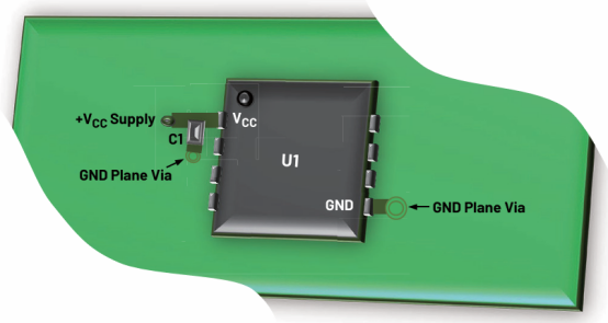
(Figure 2: Decoupling Techniques for Power Pins)
Once component placement and floorplanning are complete, another critical design aspect to address is the board layer stackup. It is highly recommended to define the layer stackup before starting PCB routing, as it determines the available return current paths for the system design.
Board layer stackup refers to the vertical arrangement of copper layers in a printed circuit board. These layers manage current and signal flow across the entire board.
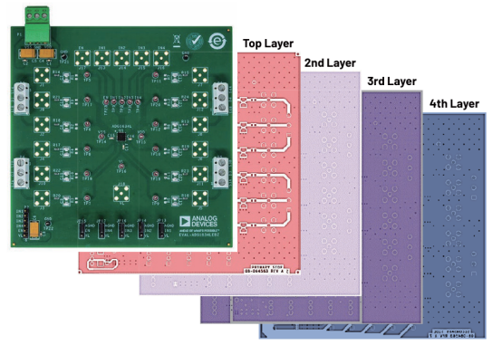
(Figure 3: Example of a 4-Layer PCB)
Figure 3 provides a visual representation of board layers. Table 1 details a typical 4-layer PCB configuration:
Table 1: Typical 4-Layer PCB Stackup
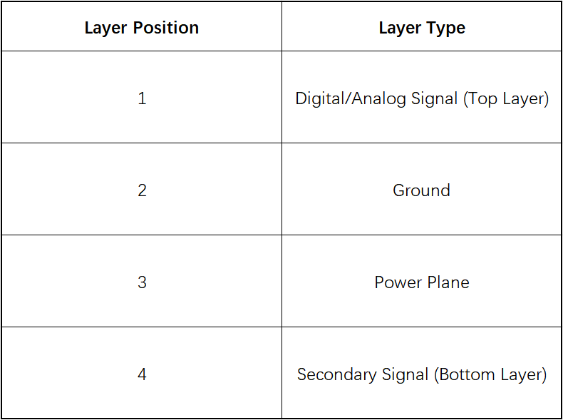
Generally, high-performance data acquisition systems require four or more layers. The top layer is typically used for digital and analog signals, while the bottom layer carries secondary signals. The second layer (ground plane) serves as the reference plane for impedance-controlled signals, reduces IR drop, and shields digital signals on the top layer. The power plane occupies the third layer.
Power and ground planes must be placed adjacent to each other, as they create additional inter-plane capacitance that aids high-frequency power supply decoupling.
Regarding ground planes, recommendations for mixed signal pcb design have evolved over the years. While splitting the ground plane into analog and digital sections was standard practice for many years, a newer approach is recommended for modern mixed-signal devices. Proper floorplanning and signal separation can effectively mitigate issues associated with high-noise signals.
Grounding is a foundational step in building a reliable mixed signal pcb. A typical 4-layer PCB requires at least one dedicated ground plane to ensure return signals follow low-impedance paths. All IC ground pins should be routed directly to the low-impedance ground plane to minimize series inductance and resistance.
In mixed-signal systems, splitting analog and digital grounds has long been a standard grounding method. However, mixed-signal devices with low digital current are better managed with a single unified ground. Ultimately, designers must evaluate which grounding approach is most suitable based on the system’s current requirements. Below is an overview of both methods.
For mixed-signal systems with a single low-digital-current ADC or DAC, a solid unified ground plane is the optimal approach. To understand the importance of a single ground layer, it is necessary to review return current behavior. Return current is the current that flows back through ground and along traces between devices to form a complete loop. To prevent mixed-signal interference, every return path must be tracked throughout the PCB layout.
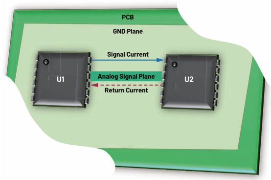
(Figure 4: Return Current in a System With a Solid Ground Plane)
The simple circuit in Figure 4 demonstrates the advantages of a unified solid ground plane over a split one. Signal current has an equal and opposite return current that flows back to the source through the ground plane, following the path of lowest impedance.
For low-frequency signals, return current follows the path of least resistance, typically a straight line between device ground reference points. For higher-frequency signals, a portion of the return current tends to follow directly beneath the signal trace. This occurs because this path offers lower impedance and creates the smallest loop area between the outgoing signal and return current.
For complex systems where a solid unified ground is impractical, split grounding may be more appropriate. The split ground plane method divides the ground plane into two sections: an analog ground plane and a digital ground plane. This approach suits more complex systems with multiple mixed-signal devices drawing high digital currents. Figure 5 shows an example of a system using split ground planes.
For systems with split ground planes, the simplest way to achieve a common reference is to bridge the gap in the ground plane and allow return currents to flow through a star ground junction. A star ground is the point where analog and digital ground planes are connected together in mixed signal pcb layout.
In typical systems, a star ground can be implemented as a narrow, continuous bridge between the analog and digital ground planes. For more complex designs, it is often implemented with a jumper resistor shunting the ground junction. Since negligible current flows through the star ground connection, high-current junctions or jumper shunts are not required. The primary function of the star ground is to ensure both grounds share the same reference potential.
Designers should always review the grounding recommendations in each device’s datasheet to ensure compliance and avoid ground-related issues. Meanwhile, mixed-signal devices with separate AGND and DGND pins can be connected to their respective ground planes, as the star ground will tie both grounds together at a single point. This arrangement ensures all high-noise digital currents flow through the digital supply to the digital ground plane and back to the digital supply, remaining isolated from sensitive analog circuitry. Isolation between AGND and DGND planes must be maintained across all layers of the multilayer PCB.
These practices align with widely accepted mixed signal pcb design guidelines for grounding implementation:
PCB layout for mixed-signal applications can be challenging, and creating a component floorplan is only the starting point. When striving for optimal performance in mixed-signal system layouts, proper board layer management and a well-defined grounding strategy are among the key points system designers must address.
Following established mixed signal pcb design guidelines helps lay the foundation for overall system integrity. Properly organized board layers support controlled current and signal flow across the board. Ultimately, selecting the most suitable grounding scheme will improve system performance and prevent issues related to high-noise signals and uncontrolled return currents.



