Previous articles have covered key technologies related to chip ESD, including ESD diodes, power clamps, CDM mechanisms, and ESD testing procedures, with a focus on chip-level electrostatic discharge protection. However, a common problem in real-world engineering applications is that an IC may pass all standard ESD tests but still suffer damage or failure when used on an actual customer circuit board.
Engineers often assume that the problem is insufficient chip-level ESD protection. However, this judgment has limitations. Not all electrical failures are caused by ESD. In many real-world applications, the underlying cause may instead be EOS (Electrical Overstress).
EOS stands for Electrical Overstress. It refers to a condition in which an IC is subjected to voltage, current, or power stress beyond its designed safe operating limits, resulting in electrical abnormalities or physical damage.
EOS can occur in many real-world application conditions, including:
EOS is not a single standardized failure test model. Instead, it is a general term for failures caused by excessive electrical stress. Any voltage, current, or power stress that exceeds the device's designed tolerance can potentially result in EOS failure.
Both ESD and EOS can cause electrical damage to an IC, which is why they are easily confused in engineering practice. However, they differ significantly in terms of stress characteristics, duration, energy, and failure mechanisms.
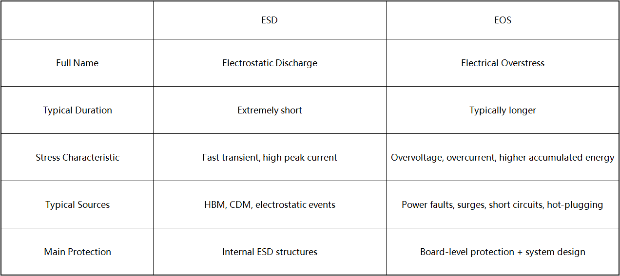
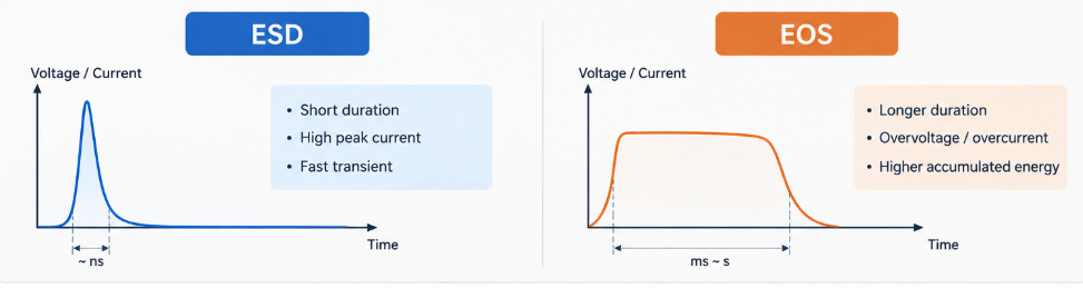
(Comparison of ESD and EOS Waveforms)
Passing standardized HBM and CDM tests only demonstrates that an IC can withstand specific short-duration electrostatic discharge stresses under defined test conditions. It does not mean that the device can withstand every type of electrical transient that may occur in a real system.
Standard ESD tests are designed around defined test models and conditions. They verify whether an IC's ESD protection structures and discharge paths can safely handle specified electrostatic pulses.
However, these tests cannot reproduce every electrical stress that may occur after the IC is integrated into a complete circuit board.
In actual circuit board applications, electrical stress may come from:
Compared with standardized ESD pulses, these events may have longer durations, higher accumulated energy, or repeated stress characteristics, resulting in different types of IC damage.
The internal ESD protection circuit of an IC is primarily designed to handle short-duration electrostatic pulses. Its purpose is to establish a controlled discharge path and divert transient energy. Therefore, passing ESD tests does not mean that an IC has system-level protection against all EOS conditions.
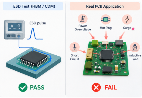
(ESD Test PASS vs Real PCB FAIL)
A common misconception in system design is that an IC can withstand all external electrical disturbances simply because its pins include an ESD protection circuit. In practice, this assumption can create significant reliability risks.
The internal ESD protection structure is an important protection layer against electrostatic events. It is designed to provide a low-impedance path for short-duration ESD currents and prevent excessive voltage from reaching sensitive internal circuits.
However, this protection is not intended to absorb large amounts of energy for an extended period. It should therefore not be treated as a substitute for system-level EOS protection.
For example, if an I/O pin is continuously exposed to a voltage beyond its specified operating range and the internal protection structure enters conduction, current may continue to flow into or through the IC.
As the stress continues, the protection device and related circuits can generate significant heat. Depending on the electrical stress and internal current path, this may eventually cause damage to components such as:
The actual damage location depends on the magnitude and duration of the external stress as well as the current path inside the IC.
A key engineering principle is that internal ESD protection is primarily intended to handle short-duration electrostatic pulses, while system-level electrical stress with significant energy should be limited and protected at the board level.
Common board-level protection methods include:
The goal is not simply to add more protection components, but to limit the voltage, current, and energy that can reach the IC and provide a controlled path for transient energy.
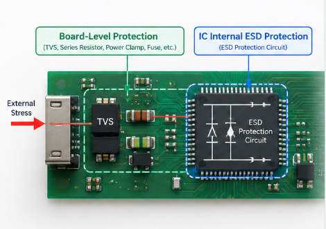
(Board-Level Protection + IC Internal ESD Protection)
EOS damage is closely related to the actual current path created by the electrical stress. Different types of stress can affect different areas of the IC:
Therefore, EOS failure analysis should not rely solely on the appearance of a localized burn mark. It is more important to trace the source of the electrical stress, current entry and exit paths, stress duration, and energy to identify the root cause.
There is no absolute method for distinguishing ESD from EOS based solely on physical failure signatures. However, practical failure analysis often reveals some characteristic differences that can be used as initial clues.
Common ESD failure characteristics include:
Common EOS failure characteristics include:
It is important to note that these failure signatures are only supporting evidence and should not be treated as final conclusions. Accurate differentiation between ESD and EOS failures requires comprehensive analysis of the failure scenario, electrical test data, application environment, test conditions, damage location, and physical analysis results.
In real-world applications, misdiagnosing an EOS failure as insufficient ESD protection can lead to an incorrect corrective strategy, wasting design resources while leaving the actual problem unresolved.
When an IC is damaged by system-level EOS, simply increasing the size of the internal ESD protection structure, strengthening the internal power clamp, or widening internal metal interconnects generally cannot solve the system-level failure.
The root cause may instead be related to board-level electrical stress, such as excessive external surge energy, improper TVS selection, continuous power supply overvoltage, load short circuits, abnormal hot-plug timing, or the lack of an appropriate freewheeling or clamping path for inductive loads.
The key risk of misdiagnosing EOS is that engineers may continue to optimize the chip's ESD protection circuit without addressing the actual source and energy path of the system-level electrical stress. As a result, the same failure may occur repeatedly.
Therefore, when investigating electrical failures in real-world applications, both chip-level and system-level factors should be considered rather than focusing only on the internal ESD structure.
When an IC experiences an electrical failure, the following factors can be checked first to avoid automatically classifying the problem as an ESD failure:
Did the failure occur during a standard ESD test or during actual customer operation? Did it occur at the moment of power-up, during cable insertion or removal, after a load short circuit, or when a motor or relay was activated?
Is the problem limited to leakage at a single I/O pin, a low-resistance path between the power supply and ground, or simultaneous abnormalities across multiple pins? Has the overall operating current of the IC changed significantly?
Was the failure caused by a short-duration transient pulse, continuous overvoltage, or overcurrent? Was there any periodic or repeated electrical stress or abnormal power sequencing?
Does the circuit board include TVS or other surge protection? Is an appropriate current-limiting circuit provided? Does the power supply have overvoltage or clamping protection? Does the grounding path provide sufficiently low impedance? Does the inductive load have an appropriate freewheeling or clamping path?
These factors can help determine whether the failure is related to system-level EOS and provide a basis for tracing the electrical stress path into the IC.
Both ESD and EOS can cause IC leakage, short circuits, functional abnormalities, and physical damage, but their stress characteristics, protection strategies, and corrective measures are significantly different. Passing standard ESD tests only verifies the IC's ability to withstand specific short-duration electrostatic pulses and does not cover every overvoltage, overcurrent, surge, hot-plugging, power reversal, or ground-bounce condition that may occur in a real system.
Therefore, when investigating an IC failure in an actual application, engineers should not determine the root cause solely based on the fact that the device passed ESD testing or on the appearance of localized physical damage. Instead, the failure scenario, electrical stress, failure location, current path, board-level protection, and physical analysis results should be considered together.
For electrical stress outside standard ESD test conditions, such as overvoltage, overcurrent, surge, hot-plugging, and inductive load transients, EOS should be considered as a potential root cause. Appropriate board-level protection can help limit the voltage, current, and energy reaching the IC and reduce the risk of application-level failure.