Summary: Combinig logic gates in projects to make new gates.
Logic gates can be combined to create other logic functions. For example, two NAND gates can form an AND gate, an AND gate followed by a NOT gate creates a NAND gate, two NOR gates can form an OR gate, and an OR gate followed by a NOT gate creates a NOR gate. These are straightforward examples for anyone with a basic understanding of logic gates.
Outside of academic examples, the practical question is: if a project needs a specific gate, why not use that gate directly? In many cases, that is the best approach. However, logic ICs come in packages containing one, two, three, or four gates. In projects that use several gates, combining available gates can sometimes eliminate the need for an additional chip.
OR and AND gates can also be built using diodes and resistors. If a project needs only one AND gate or one OR gate, a few diodes and a resistor may be enough to create it. The following examples are taken from my current shared projects.
A spreadsheet prgoam like Excel can be used to create a truth table to test diffenrt confiragtions of logic gate. Here are two examples.
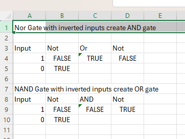
AND Gate Example
=NOT(A4) =OR(B4,B5) =NOT(C4)
=NOT(A5)
OR Gate Example
=NOT(A9) =AND(B9,B10)=NOT(C9)
=NOT(A10)
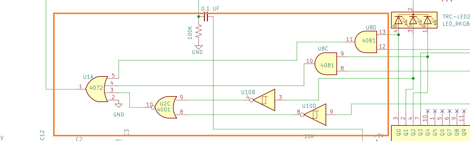
Three AND gates feed an OR gate. This example is from my reaction game project. OR gate U1A is driven by two AND gates: NOR gate U2C and NOT gates U10B and U10D combine to form the third AND gate. U10B and U10D are Schmitt trigger inverters; they are not required for this circuit but are used because three Schmitt trigger inverters are used elsewhere in the design.
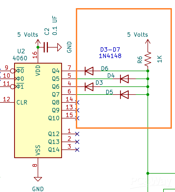
A diode AND gate: This example is from my LED Ring Clock project. D6, D5, D4, D3, and R6 form an AND gate.
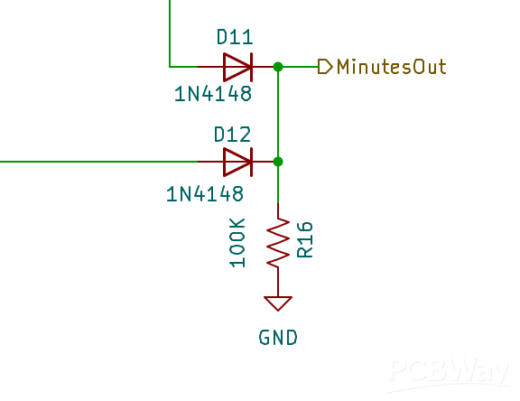
A diode OR gate: This example is from my LED Ring Clock project. D12, D11, and R16 form an OR gate.