
|
|
KiCad 10kicad
|
wfandfmeet
# Glitchwave 567 — PCBWay ordering guide (rev 0.2, 2026-07-29)
> **✅ HOLD CLEARED (2026-07-29).** The enclosure fit conflict (pot knobs
> buried under PC-pin stomp mounting) is fixed by swapping RV1–RV6 to
> ALPS RK09K1130A70 (30mm shaft, same footprint, LCSC C351173) — BOM-only
> change, no board rework. See `hardware/ENCLOSURE_FIT.md`. Cleared to
> order.
> **♻️ FAB PACKAGE REGENERATED 2026-08-02.** The gerbers/drill/pos in this
> folder were last built 2026-07-25 and had gone **stale** — four rounds of
> board changes since then (input-jack move, output-jack clearance fix,
> control-board stack header moved to B.Cu, MP1584 exposed pad connected)
> were **not** in them. Anything ordered from the old package would have
> built the July board. Everything except the drill template is now
> regenerated from the current `.kicad_pcb` files by
> `hardware/review/tools/make_fab.ps1` — **re-run that script after any
> board edit, and check the file dates here against the `.kicad_pcb` dates
> before you order.**
> **⛔ DO NOT USE THE ENCLOSURE DRILL TEMPLATE.** `drill_template_1to1.pdf`
> is dated 2026-07-25 and is **wrong**: the input jack J1 moved +3.5 mm in
> x on 2026-07-31 to clear the buck inductor. The file has been renamed to
> `drill_template_1to1.STALE_2026-07-25_DO_NOT_USE.pdf`. A fresh template
> must be produced before any enclosure is drilled. This does not block the
> PCB order — it is not a fab deliverable.
> **✅ PRE-ORDER BLOCKERS CLEARED 2026-08-02.** Four things were resolved:
> 1. **Stomp path: PC-pin variant.** No board cutouts are needed — ENCLOSURE_FIT's
> two 27 × 14.5 mm cutouts were only required on the wire-lead path.
> 2. **CONTROL board now has its four M3 standoff holes** at (17, 9.5), (121, 9.5),
> (17, 108.5), (121, 108.5) — Ø3.2 mm NPTH, ≥3.69 mm to the nearest copper and
> ≥5.5 mm to the board edge. ENCLOSURE_FIT required these ("control-board retention
> must come from standoffs") and they had never been added. MAIN board deliberately
> has none: six jack bushings with nuts through the walls retain it.
> 3. **Board-to-board connector chosen** — see the assembly notes below.
> 4. **BOM is complete.** Every line on both sheets now carries a real, orderable
> part number; the 64 lines that said `generic` were backfilled.
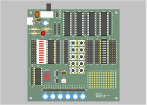
Two boards, one enclosure (Hammond 1590XX). Order both as **4-layer, full
turnkey assembly**. Gerbers/drill/pos live next to this file; BOMs are the
sheets of `hardware/BOM.xlsx` (MAIN = 297 lines, CONTROL = 22 lines).
## Board specs (both boards identical stackup)
| Parameter | Value |
|---|---|
| Layers | 4 — F.Cu route / In1 solid GND plane / In2 route / B.Cu route |
| Size | 138 × 114 mm, corner notches 11 × 11 mm (in Edge.Cuts) |
| Thickness | 1.6 mm, 1 oz copper all layers |
| Min track / clearance used | 0.25 mm / 0.13 mm (PCBWay standard 5/5 mil capable) |
| Vias | 0.5 mm pad / 0.3 mm drill, min hole-to-hole 0.25 mm |
| Finish | HASL lead-free is fine (ENIG optional) |
| Mask / silk | Any color Jason likes; silk clipping over pads is expected |
DRC status (KiCad 10, **re-run 2026-08-02 against the current boards**):
**0 unconnected, 0 shorts, 0 clearance violations, 0 schematic-parity errors**
on both boards. MAIN = 72 warnings + 4 courtyard errors; CONTROL = 6 warnings,
0 errors. The 4 courtyard errors are the same shallow decoupling-cap kisses
(≤0.4 mm, bodies verified clear) — no action needed.
## Turnkey sourcing notes
1. **LCSC parts** — every BOM line carries an LCSC C-number (stock verified
2026-07-25; pot line updated 2026-07-29). Pots: ALPS RK09K1130A70
(C351173) ×6, B10k linear, snap-in, 30mm shaft.
2. **Stomp switches SW1/SW2 — mark DNP, do NOT ask PCBWay to source them.**
Suntsu SSWFS-S01-AC09-HWH is a Digi-Key *Marketplace* listing, Mouser has
no listing for it or its wire variant, and has no foot-switch
category at all** — no fab-side distributor stocks this class of part.
It is a commodity pedal-industry switch: Amplified Parts **P-H604**
publishes matching dimensions (12 mm × 1 mm bushing, 14.3 mm long, body
25.3 × 12.6 mm) against this footprint's Ø12.2 hole and 25.5 × 13 body,
and Love My Switches stocks PCB-mount ($3.99) and pre-wired ($5.75)
versions. Buy them direct and fit them at final assembly. This takes the
only unsourceable line off the fab order's critical path.
⚠️ Two numbers still unverified: the below-panel body depth (ENCLOSURE_FIT
assumes 15.0 ± 1.0 mm — measure a real one before cutting metal), and the
footprint `descr` says thread "15/32-32" while ENCLOSURE_FIT and Amplified
Parts both say M12 × 1.0. The Ø12.2 clearance hole suits either; the nut
does not.
3. **Raspberry Pi Pico (U20)** — the official Pico module, SMD-mounted flat
(castellated edge pads, official land pattern). PCBWay can source it or
Jason can consign two.
4. **DNP parts** — LFIL/OFIL cap pads near the LM567 are intentionally
unpopulated ("the voice" of the pedal). They are marked DNP in the BOM.
Do not let the fab "helpfully" populate them.
## Assembly notes
- CONTROL board: pots, stomps, and WS2812 LEDs mount on F.Cu; the 2×8 keyed
stack header (**ref is J1 on the control board**) mounts on **B.Cu** — this
is now true in the board file as of 2026-08-02; until then it was drawn on
F.Cu, where it could not have mated. It uses a project-specific
**pre-mirrored** footprint, `PinHeader_2x08_P2.54mm_Vertical_Mirrored`,
which cancels KiCad's flip so pin N lands on pin N of J10 below. Verified
16/16 pads and 16/16 nets against J10. **Do not substitute the stock
PinHeader_2x08 footprint on this part** — flipping the stock one permutes
the pin numbers (1↔15, 2↔16, 3↔13, …) and reverses the whole connector.
Same header on MAIN (J10) mounts topside at (96, 104) — only DC nets cross.
**The pair is now chosen and gives exactly the 11.00 mm gap the enclosure needs:**
| Board | Half | Part | LCSC | Key dimension |
|---|---|---|---|---|
| MAIN, J10, **top** side | female socket | XFCN **PM254V-12-16-H85** | C46595985 | body **8.50 ±0.15 mm** |
| CONTROL, J1, **bottom** side | male header | XFCN **PZ254V-12-16P** | C492425 | insulator **2.50 mm**, mating pin 6.0 ±0.20 mm |
2.50 + 8.50 = **11.00 mm**, plastic face to plastic face — a positive mechanical
stop, not a nominal. Worst-case tolerance 10.70–11.30 mm. The 6 mm pin sits inside
the socket's 3.68–6.35 mm insertion-depth window and does **not** bottom out, which
is what makes the plastics the datum. Verified against both manufacturers' drawings;
the two datasheets name each other as the mate.
⚠️ **Do not substitute a long-pin or "stacking" header** (e.g. 13.5 mm pins). It
would exceed the socket's maximum insertion depth, bottom out internally, hold the
plastics apart and leave the gap indeterminate.
⚠️ **The socket goes on MAIN deliberately.** MAIN carries the DC jack, so its half is
live whenever power is applied — recessed socket contacts can't be shorted by a
dropped screw or a probe, 16 exposed pins at 18 V can. It also puts the lighter half
on the board that hangs upside down.
- MAIN board: wall-mounted jacks (2× PJ-603A, 3× PJ-3410, 1× DC-044A) are
right-angle parts hanging off board edges — verify they sit flush before
wave/hand solder.
- First-article checklist is the README sheet inside `BOM.xlsx` — run it
before boxing the assembled boards.
## Suggested order
Qty 5 of each board, turnkey, lead-free HASL, any-color mask.
The enclosure drill template is **not** in this package any more — the old one
was quarantined as stale (see the warning at the top of this file). It was never
a fab deliverable, only a 1:1 print for Jason's drill press, so its absence does
not affect the PCB order. A new one must be generated before any metal is cut.
wfandfmeet
Project images are for reference only. Actual production is based on the manufacturing files on the project page.
Please review the designer's notes (e.g., PCB thickness) and select the appropriate options.
PCBWay is not responsible
for issues caused by unsuitable parameter selections.
For more important ordering information, please refer to
Read More

- ✖ | No sharing or redistributing in any way of the 3D files or derivatives
- ✖ | No remixing
- ✖ | Non-commercial Use (only for personal use)


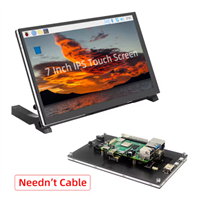
Raspberry Pi 5 7 Inch Touch Screen IPS 1024x600 HD LCD HDMI-compatible Display for RPI 4B 3B+ OPI 5 AIDA64 PC Secondary Screen(Without Speaker)
BUY NOW

- Comments(0)
- Likes(0)
 More by Engineer
-
Programmable Mist Maker - XIAO / QT PY Extension
1185 2 1 -
RadioHAT - Raspberry Pi radio development platform
991 0 2 -
-
-
-
-
ARPS-2 – Arduino-Compatible Robot Project Shield for Arduino UNO
3406 0 6 -
A Compact Charging Breakout Board For Waveshare ESP32-C3
4033 3 8 -
AI-driven LoRa & LLM-enabled Kiosk & Food Delivery System
4425 2 2