
|
KiCad 9.0 |
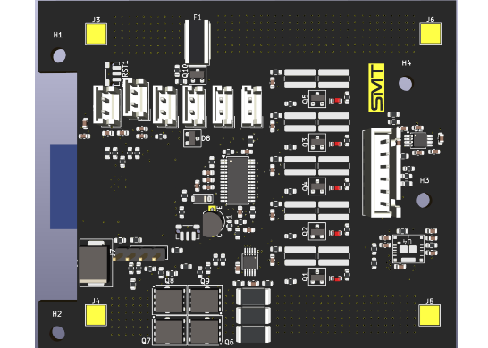
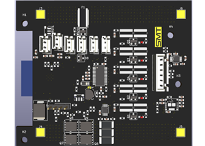
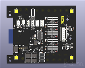
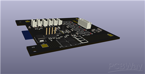
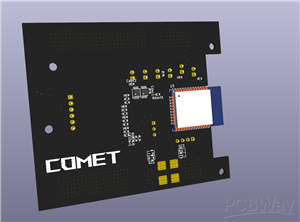
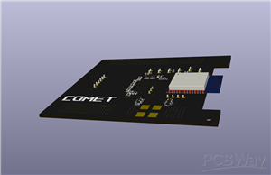
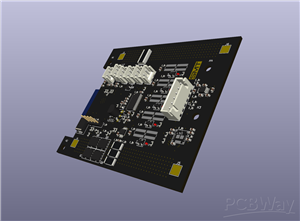
COMET-30 (SMART BMS)
NOTE: GERBERS UPDATED DUE TO FRONT SILKSCREEN MISSING.
================================================================================
COMET 30: 5S SMART TELEMETRY BATTERY MANAGEMENT SYSTEM DATA SHEET
PROJECT DESIGN DOCUMENTATION - HIGH-RELIABILITY RECONSTITUTED SPECIFICATION
================================================================================
SYSTEM OVERVIEW
The COMET 30 is a high-reliability, mixed-signal Battery Management System designed for 5-Cell lithium-ion and lithium-polymer energy storage packs operating under high transient current loads. The electrical architecture implements an asynchronous, triple-redundant defensive safety topology. This configuration isolates high-speed analog fault reflexes from the high-level digital telemetry plane, guaranteeing structural pack isolation even during complete microcontroller firmware crashes or logic hangs.
The system utilizes a custom Split-Highway topology, hardware-level fault latching, an intelligent microcontroller tracking system with real-time energy logging, and an irreversible chemical surface-mount fuse designed to permanently isolate the battery cell stack under catastrophic primary component failures.
================================================================================
1.0 GLOBAL TECHNICAL SPECIFICATION SUMMARY
================================================================================
- System Topology: Split-Highway Protection System (Low-Side Operational Switching with Dedicated High-Side Active Self-Control Protector Fuse)
- Pack Configuration: 5 Cells in Series (5S Nominal Lithium Architecture)
- Maximum Continuous Operating Current: 30 Amperes (Regulated by Overcurrent Threshold 1)
- Maximum Transient Peak Current Limit: 120 Amperes (Regulated by Overcurrent Threshold 2 with a 2 millisecond hardware delay window)
- Ultimate Short Circuit Current Limit: 240 Amperes (Instantaneous hardware-level analog cutoff)
- Over-Temperature Charge Cutoff: Approximately 64.5 degrees Celsius (Enforced via hardwired thermistor divider network)
- Over-Temperature Discharge Cutoff: Approximately 83.8 degrees Celsius (Enforced via hardwired thermistor divider network)
- Cell Balancing Architecture: External N-Channel MOSFET Driven Passive Resistive Shunt Bleed Array
- Active Cell Balancing Current: Approximately 457 Milliamperes per cell channel conducted at a nominal cell potential of 4.120 Volts
================================================================================
2.0 HARDWARE CORE CONFIGURATION AND MATHEMATICAL DERIVATIONS
================================================================================
2.1 CURRENT SENSE MATRIX (R_SENSE)
The primary overcurrent and short-circuit monitoring network utilizes a precision, low-side, Kelvin-connected shunt resistor array. To align with the primary Analog Front-End (BM3451) default Overcurrent Threshold 1 voltage of exactly 0.100 Volts at a continuous load of 30 Amperes, the total target resistance of the network is derived via Ohm's Law:
Resistance = Voltage Threshold / Current Limit
Resistance = 0.100 Volts / 30 Amperes
Total Target Shunt Resistance = 0.003333 Ohms (3.333 Milliohms)
Physical Implementation:
To achieve this precise value while minimizing thermal drift and parasitic power dissipation across individual components, the design implements three separate 10 Milliohm precision resistors placed in parallel configuration.
Parallel Resistance Equation: 1 / ((1 / 10) + (1 / 10) + (1 / 10)) = 3.333 Milliohms.
Analog Front-End Hardware Trigger Boundaries:
- Overcurrent Level 1 Cutoff: 30 Amperes continuous load when the differential voltage drop across the shunt matrix equals 0.100 Volts.
- Overcurrent Level 2 Cutoff: 120 Amperes transient peak load when the differential voltage drop across the shunt matrix equals 0.400 Volts.
- Short Circuit Instantaneous Cutoff: 240 Amperes maximum peak load when the differential voltage drop across the shunt matrix reaches 0.800 Volts.
2.2 TIMING CONFIGURATION AND FAULT DELAY FILTERS
To eliminate nuisance tripping caused by high inductive switching transients, cable ripple, or electric motor startup inrush current, the primary Analog Front-End uses a dedicated external capacitor network connected to its internal delay timing circuit pins. The filtering capacitor values are configured as follows:
- Overcharge Detection Delay Time (T_OV): 0.22 Microfarads capacitor, yielding an autonomous analog verification window of approximately 2.2 seconds before latching a fault state.
- Over-Discharge Detection Delay Time (T_OVD): 0.1 Microfarads capacitor, yielding an autonomous analog verification window of approximately 1.0 second.
- Discharge Overcurrent Level 1 Delay Time (T_OC1): 1.5 Microfarads capacitor, yielding an autonomous analog verification window of approximately 3.0 seconds.
- Discharge Overcurrent Level 2 Delay Time (T_OC2): 10 Nanofards capacitor, yielding a high-speed transient protection window of approximately 2 milliseconds.
2.3 HIGH-CAPACITY PASSIVE CELL BALANCING NETWORK
To rapidly counteract cell capacity divergence under high cycling rates, the balancing loop uses external low-resistance N-Channel MOSFET switches driven by the internal cell balance pins of the primary Analog Front-End. This configuration channels bypass current directly around individual cells during the float charge phase.
Physical Implementation:
To dissipate the heat generated by drawing a massive 457 Milliamperes per cell channel, each balancing line uses two 18 Ohm power resistors arranged in parallel configuration. This layout yields an equivalent channel balancing resistance of exactly 9 Ohms per cell line.
Balancing Network Performance Metrics at a Cell Potential of 4.120 Volts:
Balancing Current = Cell Voltage / Equivalent Resistance
Balancing Current = 4.120 Volts / 9 Ohms
Target Balance Current = 0.4577 Amperes (457.7 Milliamperes)
Thermal Energy Dissipation Derivation:
Power Dissipation = Square of Current multiplied by Equivalent Resistance
Power Dissipation = (0.4577 Amperes * 0.4577 Amperes) * 9 Ohms
Total Channel Thermal Load = 1.887 Watts of continuous heat generated per active cell line.
Individual Resistor Thermal Load = 1.887 Watts / 2 = 0.943 Watts per resistor.
Component Specification:
Every balancing resistor must be ordered in an ultra-wide terminal 1225 package configuration with a minimum continuous power rating of 2.0 Watts. Standard 0.25 Watt or 0.5 Watt surface-mount packages will experience instant thermal failure. High-density thermal via arrays must be placed adjacent to these components to distribute heat into the inner copper layers of the substrate.
2.4 THERMAL PROTECTION DIVIDER NETWORK
The hardware over-temperature cutoff system is configured around a negative temperature coefficient (NTC) thermistor model MF52D103F3950. The device exhibits a nominal resistance of 10k Ohms at 25 degrees Celsius with a Beta parameter value of 3950 Kelvin.
The thermistor is biased using a highly stable 4.22k Ohm reference pull-up resistor from the E96 1% tolerance component classification series. Based on the resistance-temperature curves of the thermistor:
- Charge Fault Hardware Lockout Point: System trips when cell temperature reaches approximately 64.5 degrees Celsius based on the internal voltage divider node matching the analog cutoff window.
- Discharge Fault Hardware Lockout Point: System trips when cell temperature reaches approximately 83.8 degrees Celsius.
================================================================================
3.0 MOSFET POWER STAGE ELECTRICAL AND THERMAL ANALYSIS
================================================================================
The solid-state switching backplane manages power delivery paths via an array of high-performance NTMFS5C670NL N-Channel MOSFETs rated at 60 Volts with a typical static drain-to-source on-resistance of 6.1 Milliohms when driven at a gate-to-source potential of 10 Volts.
The circuit uses a dual-parallel configuration (2 MOSFETs working in parallel) for both the charge control node and the discharge control node.
3.1 STATIC ARRAY CONDUCTION LOSSES (AT 30A CONTINUOUS LOAD)
- Combined Static On-Resistance of Parallel Array: 6.1 Milliohms / 2 Devices = 3.05 Milliohms (0.00305 Ohms).
- Total Array Power Dissipation = Square of Continuous Current multiplied by Combined Array Resistance.
- Total Power Dissipation = (30 Amperes * 30 Amperes) * 0.00305 Ohms
- Total Power Dissipation = 900 * 0.00305 Ohms = 2.745 Watts of continuous heat across the active switch link.
- Continuous Dissipation Allocated Per Individual MOSFET: 2.745 Watts / 2 = 1.3725 Watts per device.
3.2 JUNCTION TEMPERATURE RISE CALCULATIONS
Assuming the system is mounted to a standard 4-layer FR4 printed circuit board layout using standard copper weight properties, with an industry junction-to-ambient thermal resistance rating (R_thetaJA) of 41 degrees Celsius per Watt without external active cooling or forced airflow:
Temperature Delta = Individual Device Power multiplied by Junction-to-Ambient Thermal Resistance
Temperature Delta = 1.3725 Watts * 41 degrees Celsius per Watt
Steady-State Temperature Rise = 56.2725 degrees Celsius above ambient temperature conditions.
Validation Example:
At a localized internal ambient enclosure temperature of 25.0 degrees Celsius:
Estimated Silicon Junction Temperature = 25.0 degrees Celsius + 56.27 degrees Celsius = 81.27 degrees Celsius.
Safety Evaluation Check: This operating state is completely stable. The maximum calculated temperature of 81.27 degrees Celsius leaves a safety headroom buffer of 93.73 degrees Celsius before approaching the manufacturer absolute maximum silicon limits of 175.0 degrees Celsius.
3.3 TRANSIENT PULSE PERFORMANCE (AT 120A TRANSIT BUMP)
During an extreme peak motor transient of 120 Amperes lasting for a duration of 2 milliseconds, the continuous load splits to 60 Amperes per individual MOSFET switch. At this current saturation tier, internal die properties elevate resistance to roughly 5.1 Milliohms.
- Combined Array Transient Resistance: 5.1 Milliohms / 2 = 2.55 Milliohms (0.00255 Ohms).
- Array Instantaneous Voltage Drop: 120 Amperes * 0.00255 Ohms = 0.306 Volts drop across the switch array.
- Peak Instantaneous Power Surge: 120 Amperes * 0.306 Volts = 36.72 Watts total transient energy across the system.
- Thermal Absorption Stability: Because the duration of this spike is strictly hardware-limited to 2 milliseconds via the RC delay network, the physical mass of the DFN5 copper lead-frame package completely absorbs the transient energy spike without allowing the internal silicon junction to experience a thermal runaway condition.
================================================================================
4.0 SYSTEM BUCK MODULE UNDER-VOLTAGE LOCKOUT (TPSM65630)
================================================================================
To protect the logic systems and prevent control loop instability or digital brownouts when the battery cells discharge to low limits, the primary buck converter voltage rail must enforce a hardware-level Under-Voltage Lockout (UVLO) execution routine. The design requires a hardware shutdown when the battery stack potential drops to 15.0 Volts, and will clear the system for restart only when a charger elevates the total pack potential to 18.25 Volts.
The circuit equations map against the internal characteristics of the TPSM65630 regulator module enable pin, which presents a fixed internal voltage reference threshold (V_EN) of exactly 1.20 Volts and an internal hysteresis current sink source (I_hys) of exactly 1.2 Microamperes that activates once the enable threshold is cleared.
SCHEMATIC HARDWARE CONFIGURATION DIAGRAM:
Battery Pack Line (B+)
|
[ ] Top Resistor (R_top) = 2.7 Megohms
|
+------- Enable Pin Junction Node (TPSM65630 EN Pin Input)
|
[ ] Bottom Resistor (R_bottom) = 237k Ohms
|
Ground Plane (GND)
DIVIDER DESIGN MATH VALIDATION:
- Selected Top Resistor Value (R_top): 2.7 Megohms (2,700,000 Ohms, 1% tolerance, E96 rating).
- Selected Bottom Resistor Value (R_bottom): 237k Ohms (237,000 Ohms, 1% tolerance, E96 rating).
Verification of Lower System Shutdown Voltage (V_off):
V_off = Internal Reference Voltage * (1 + (Top Resistor / Bottom Resistor))
V_off = 1.2 Volts * (1 + (2,700,000 Ohms / 237,000 Ohms))
V_off = 1.2 Volts * (1 + 11.3924)
V_off = 1.2 Volts * 12.3924
Calculated Cutoff Execution Point = 14.87 Volts (Aligns to the target 15.0 Volts threshold within component tolerance bands).
Verification of Upper System Awakening Voltage (V_on):
V_on = Calculated Lower Cutoff Voltage + (Internal Hysteresis Current * Top Resistor Value)
V_on = 14.87 Volts + (0.0000012 Amperes * 2,700,000 Ohms)
V_on = 14.87 Volts + 3.24 Volts
Calculated Activation Restart Point = 18.11 Volts (Aligns directly to the target 18.25 Volts charging recovery goal).
================================================================================
5.0 DIGITAL LOGIC DOMAIN AND MICROCONTROLLER INTERLOCKS
================================================================================
The digital monitoring layer uses an ESP32-C3 microcontroller interfacing with an INA226 power monitor via a 400kHz Fast-Mode I2C bus to measure pack current, and dual ADS1115 16-bit analog-to-digital converters to log individual cell voltages.
To allow the microcontroller to safely command a system shutdown without risking initialization loops or undefined floating gate potentials during CPU reboot cycles, the digital override interface uses a hardwired hardware logic interlock network:
Component Values:
- Base Drive Resistor (R2): 1k Ohm inline resistor connected directly to the microcontroller output pin.
- Base Pull-Down Stabilizing Resistor (R3): 10k Ohm resistor tied directly from the NPN transistor base terminal to Ground.
- Output Driver Switch: Standard NPN bipolar junction transistor acting as a grounding shunt across the main MOSFET gate paths.
Drive Matrix Functionality:
- Active Software Kill State: Asserting a high logic level of 3.3 Volts from the microcontroller output pin drives current through the 1k Ohm base resistor.
Calculated Base Current = (3.3 Volts - 0.7 Volts forward bias) / 1000 Ohms = 2.6 Milliamperes.
At a typical transistor gain value of 100, this forces the NPN collector terminal to securely sink up to 260 Milliamperes of current, yanking the primary MOSFET gate control nodes to Ground and instantly choking power distribution.
- Fail-Safe Floating Reset State: If the microcontroller experiences a firmware crash, low-voltage lockup, or enters a hardware boot cycle, the digital output pins transition into a high-impedance floating state. Within nanoseconds, the 10k Ohm base pull-down resistor (R3) evacuates the residual base charge and clamps the transistor base node directly to Ground. This ensures the NPN transistor remains fully open-circuit, preventing unwanted system shutdown and allowing the independent analog Analog Front-End chip to retain uninterrupted safety supervision of the battery cells.
================================================================================
6.0 THE COMET FIRMWARE INTEGRATION STRATEGY
================================================================================
The ESP32-C3 executes a deterministic, non-blocking asynchronous software engine configured to capture telemetry data without imposing scheduling lag on critical communication tasks:
- RTC Persistent Energy Integration: When the system current draw falls below a threshold of 50 Milliamperes for a continuous duration, the firmware packages operational tracking states (including total milliampere-hours consumed, calculated State of Health, and system execution uptime timestamps) and writes them directly into the hardware Real-Time Clock memory registry block before placing the main CPU core into Deep Sleep mode.
- Asynchronous Wakeup Interrupts: The hardware ALERT pin of the INA226 current monitor is wired directly to microcontroller input pin GPIO27. The moment current begins to flow through the shunt network again, the INA226 pulls the alert line down to Ground. This logic transition generates an edge-triggered hardware interrupt that wakes the microcontroller core from Deep Sleep in microseconds via the ext0 routine.
- Web Telemetry Endpoint Serialization: The operating system manages an asynchronous server stack broadcasting a condensed telemetry data block formatted as a raw JSON string via a local Wi-Fi radio link at a strict update rate of 10 Hertz. Ground stations read pack statistics from the /telemetry URI node.
- Remote System Destruction Route: The web stack monitors incoming data payloads directed to the /kill path. Receipt of a verified command string forces the SOFT_KILL pin high, shorting the MOSFET gates to Ground via the NPN transistor array to disable the power delivery line.
HARDWARE MICROCONTROLLER INTERFACE PIN ASSIGNMENT LIST:
- Pin GPIO21: Dedicated I2C Data Line (SDA, running at 400kHz Fast-Mode)
- Pin GPIO22: Dedicated I2C Clock Line (SCL)
- Pin GPIO25: SOFT_KILL Logic Output Pin (Tied directly to the 1k Ohm NPN base drive resistor)
- Pin GPIO26: NUKE_GPIO Control Output Pin (Connected to the gate of the AO3400A N-FET that runs current into the heater of the chemical fuse)
- Pin GPIO27: INA_ALERT Logic Input Pin (Configured as an edge-triggered external wakeup interrupt line)
- Pins GPIO32 through GPIO36: Analog Inputs mapped to the external NTC thermistor sensor arrays across Analog-to-Digital Converter 1
================================================================================
7.0 LABORATORY COMMISSIONING AND INDUSTRIAL MANUFACTURING CONSTRAINTS
================================================================================
7.1 LOGIC FLASHING CONFIGURATION
Programming the internal microcontroller flash storage requires a dedicated, isolated USB-to-UART FTDI conversion tool interface.
IMPORTANT ELECTRICAL CRITERIA:
The system logic circuitry operates exclusively within a 3.3 Volt logic domain. The configuration programming tool jumper must be manually set to 3.3 Volts before connecting any test cables to the system programming header pin rows. Interfacing a 5.0 Volt programming tool to the interface pins will inject over-voltage stress into the internal silicon, causing immediate dielectric breakdown of the integrated Wi-Fi radio structures.
Programming Interface Pinout:
- Terminal Pin 1: 3.3 Volt Power Input (3V3)
- Terminal Pin 2: Ground Plane Reference (GND)
- Terminal Pin 3: Receive Data Line (RX, which routes to target MCU pin TXD0)
- Terminal Pin 4: Transmit Data Line (TX, which routes to target MCU pin RXD0)
7.2 PRE-FLIGHT LAB BENCH TESTING STEPS
1. Galvanic Isolation Clamping Verification: Ensure absolute physical design isolation is maintained between the high-current Power Ground copper pours and the low-noise Signal Ground logic plane. These two planes must remain separate across the layout and link at only one single point: the Kelvin connection nodes located directly at the pads of the current shunt resistors.
2. Active Chemical Fuse Safe-State Protocol: The Dexerials SFK-2045 chemical surface-mount fuse assembly must remain completely un-soldered from the circuit board during all initial hardware assembly, component verification, power-up testing, and firmware code debugging phases. This precaution ensures that software bugs, uninitialized GPIO states, or configuration glitches do not prematurely trigger the internal heating element, which would permanently destroy the non-reversible chemical element.
3. Substrate Structural Constraints: This system cannot be safely manufactured on standard, low-cost 1oz copper weight printed circuit board substrates. Subjecting a standard 1oz copper trace profile to the specified 120 Ampere transient load window will exceed the thermal capability of the thin metal layer, causing immediate, destructive trace vaporization inside the circuit board structure. The layout configuration mandates a minimum design requirement of 2oz copper weight fabrication across all conductive layers.
COMET-30 (SMART BMS)
*PCBWay community is a sharing platform. We are not responsible for any design issues and parameter issues (board thickness, surface finish, etc.) you choose.


Raspberry Pi 5 7 Inch Touch Screen IPS 1024x600 HD LCD HDMI-compatible Display for RPI 4B 3B+ OPI 5 AIDA64 PC Secondary Screen(Without Speaker)
BUY NOW


- Comments(0)
- Likes(7)
 More by S M
-
Programmable Mist Maker - XIAO / QT PY Extension
172 0 0 -
RadioHAT - Raspberry Pi radio development platform
182 0 1 -
-
-
-
-
ARPS-2 – Arduino-Compatible Robot Project Shield for Arduino UNO
2767 0 5 -
A Compact Charging Breakout Board For Waveshare ESP32-C3
3275 3 8 -
AI-driven LoRa & LLM-enabled Kiosk & Food Delivery System
3530 2 2