The purpose of package
ICs, unlike resistors and capacitors, require a higher level of protection, electrical connections, and heat dissipation. To meet these needs, IC packages serve a crucial role. These packages not only safeguard the ICs from environmental factors but also provide the necessary electrical connections and heat dissipation. In addition, IC packages can offer additional features such as hermeticity, lead-free solder, and RF shielding.
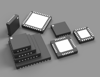
Figure 1: QFN Package
QFN stands for Quad Flat No-leads. It is characterized by its square or rectangular shape and the absence of leads. A QFN package mainly consists of the bond wire, lead frame, silicon die, exposed pad, die-attach, and mold compound. Among them the silicon die, the lead frame, and the solder pads are three crucial components. The die is the actual integrated circuit chip, and it contains the electronic circuitry of the IC. The lead frame provides electrical connections between the die and the rest of the QFN structure, and the solder pads are used to connect the package to the circuit board, improving the package's thermal performance, particularly for discrete devices.
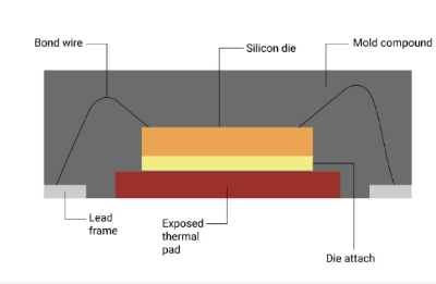
Figure 2: Structure of QFN Package
Advantages of QFN packages
QFN packages offer several advantages that make them highly desirable in various electronic applications. They excel in thermal performance due to the exposed thermal pad on the bottom. Their compact size and absence of leads make them space-efficient, ideal for space-constrained devices. QFN packages also exhibit improved electrical performance with shorter electrical paths and lower inductance. Additionally, they comply with lead-free regulations, and are easy to handle during assembly, streamlining the manufacturing process.
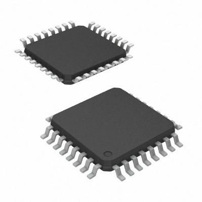
Figure 3: QFP Package
QFP packages also have a square or rectangular shape, but unlike QFN packages, they feature gull-wing or J-shaped leads extending from all four sides of the package, providing electrical connections to the circuit board. Additionally, QFP packages are known for accommodating a higher number of input and output pins compared to QFN packages due to the increased lead count. This makes QFP packages suitable for applications requiring a more extensive range of input and output connections.
QFN vs. QFP: Selecting the Appropriate Package
If space on the PCB is limited, and compact size is essential, QFN packages might be preferred due to their absence of leads and smaller footprint. On the other hand, if the component requires a higher pin count and wider lead spacing, QFP packages would be more suitable. Thermal considerations, soldering techniques, and assembly processes also play a role in determining the optimal package for a particular application.


