High-density interconnect (HDI) technology allows printed-circuit board (PCB) designers to increase routing density, reduce layer count, and improve the thermal and electrical characteristics of their board designs. This approach uses advanced via technology to combine two conventional eight-layer cards into a single 18-layer HDI card. The cards can use their own power supplies or share a redesigned one, creating a product that is 50% smaller.
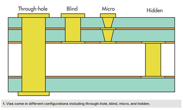
PCB vias come in different configurations (Fig. 1). Through-hole (TH) vias originate and terminate at the outer layers of the PCB, while blind vias originate on an outer layer and terminate on an inner layer. Buried vias are completely buried within the board, connecting only inner layers and not reaching the outer layers at all. Microvias are a form of blind vias that penetrate only one or two layers, and they have an extremely small drill hole (from 0.008 in./0.2 mm all the way down to 0.004 in./0.102 mm).
In addition to using microvias, blind vias, and buried vias, this technique requires careful electromagnetic interference (EMI) and thermal analysis, PCB layer stackup, and power/signal/ground distributions. When combined, the two cards look like Figure 2. To combine the boards, you’ll need to:
• Ensure that the on-board power supplies can be split evenly between the two eight-layer sections, or newly designed power supplies for two cards are in place
• Change all through-hole parts to surface-mount (SMT) parts, and change the placement to single-sided
• Mirror and combine the card layouts, so layer 1 to layer 8 is the first card and layer 11 to layer 18 is the second.
• Use blind vias or buried vias for the power and ground nets that connect to or cross layers 9 and 10

You’ll also need to be sure that when you place the ball-grid array (BGA) components that require decoupling capacitors that there is space for the capacitors on the mirrored locations underneath those BGA packages.
In addition, if a completely new layout design for the conventional card is permitted (beyond the changes described above), the two cards can be designed back-to-back directly. In that case, the bottom sides of the two cards would be layer 9 and layer 10 after the combination. This would yield a single 16-layer HDI board over two eight-layer conventional boards.


