
|
KiCad 9.0 |
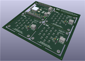
Lab Bench & Hardware Diagnostic Toolkit
Auralab_Workstation
Advanced 4-layer PCB design featuring split-plane noise isolation (AGND/DGND) and asynchronous dual-core processing. Implements a handheld multi-tool oscilloscope, current tracker, and symmetrical DC power supply.
AURALAB WORKSTATION: Pocket-Sized Lab Bench & Hardware Diagnostic Toolkit
An Open-Source Multi-Function Tool Engineered for the 2026 KiCad PCB Design Contest
Executive Summary & Architectural Overview
The Auralab Workstation (also referred to as the Pocket-Sized Workstation) is an ultra-portable, all-in-one hardware test, measurement, and diagnostic platform designed entirely within KiCad E.D.A. 9.0.7. Built upon the dual-core ARM Cortex-M0+ RP2040 microcontroller , this instrument replaces a bench worth of bulky test equipment, providing a 12-bit Oscilloscope , a Programmable bipolar ±15V Bench Power Supply , an automated Component Curve Tracer , and a Smart Hardware Safety / Fault Interrupter inside an affordable, pocket-sized PCB form factor.
Core System Functionalities & Operation Modes
1. Oscilloscope Mode
Purpose: Provides real-time signal visualization and automatic parametric waveform estimation directly on an integrated TFT display.
Signal Path Execution: BNC/Coaxial input signals pass through an AC/DC coupling selector switch and an high-impedance buffer. A high-speed, SPI-driven MCP3201 12-Bit SAR ADC digitizes the signal, feeding raw telemetry into the RP2040.
Extracted Metrics: Real-time computation on the RP2040 extracts key signal attributes, including frequency, duty cycle, time period, peak-to-peak voltage (Vpp), and RMS values.
2. Bipolar DC Benchtop Power Supply Mode
Purpose: Functions as a precision-adjustable power supply delivering split rails up to ±15V to external prototype circuits via low-impedance screw terminals.
Control Loop Execution: An incremental rotary encoder registers precise user inputs, which are processed by the microcontroller to reconfigure an MCP42010 dual digital potentiometer. The digital pot dynamically alters the feedback network of a TPS65131 split-rail converter , enabling real-time, software-calibrated output voltage control across the screen terminal interface.
3. Automated Component Tester & Curve Tracer Mode
Purpose: Traces and plots characteristic Voltage vs. Current (V-$I$) profiles of un-biased, two-terminal components (diodes, BJTs, resistors, LEDs) directly to the TFT screen.
Execution: The system sweeps voltages internally using a software-generated Sweep PWM filtered output amplified through a dedicated Programmable Voltage Sweep Amplifier (TL072). Concurrently, real-time current draw is measured via a shunt resistor network. The resulting V-$I$ trace exposes vital silicon parameters including minimum threshold voltages (Vth), linear/triode regions, saturation, and cutoff points.
4. Smart Fault Detection & Hardware Overload Interrupter
Purpose: Acts as an ultra-fast hardware protection suite that scans for shorts, continuity, or out-of-bounds voltage/current surges.
Execution: A dedicated dual-range ammeter circuit monitors incoming line conditions. If current consumption exceeds user-defined limits, an internal hardware flag (CURRENT_ALERT) triggers. The system immediately alerts the user visually through a high-intensity ALERT_LED and acoustically through a resonant Buzzer Circuit. Critically, the software and hardware isolation structures instantly cut off terminal paths to protect both the user's external circuit and the internal hardware layers of the Auralab Workstation itself.
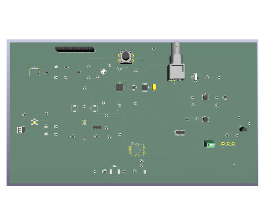
Detailed Schematic Breakdown, Hardware Architecture & Footprints
The system architecture is compartmentalized into three primary, highly optimized schematic modules:
Module 1: Power Management & Filtration (Sheet 2/4)
This module regulates raw input power, structures battery charging profiles, and handles the generation of high-efficiency analog and digital operational rails.
USB Input & Protection Subsystem: Uses a robust 16-pin USB Type-C receptacle (USB_C_Receptacle_USB2.0_16P). Ground loops and electrostatic shock hazards are nullified via an ultra-low capacitance USBLC6-25C6 ESD protection array tied across the D+/$D-$ differential signaling lines.
Filtration and Inrush Control: Input voltage passes through a reset-capable Polyfuse (F1) and an MBR0520 Schottky diode (D4) for reverse-polarity protection. A high-impedance Ferrite Bead (FB1) suppresses high-frequency switching noise before distributing power to the system rails (+5V_RAW).
Lithium-Ion Battery Management System (BMS): Integrates a TP4056-42-ESOP8 linear charger (U8). Charge current is programmed to a safe, sustainable threshold using a precision 1.2kΩ resistor (Rprog). Status LEDs provide immediate visual telemetry on battery charging state (RED_LED for charging , GREEN_LED for standby/fully charged ).
3.3V Digital Regulator: An AP2112K-3.3 low-dropout linear regulator (U7) steps down the primary voltage vector to establish a clean, low-ripple +3V3_DIGITAL rail , stabilized with low-ESR 10μF ceramic smoothing capacitors.
Split-Rail Converter: The core of the variable bench supply relies on a TPS65131RGE split-rail buck-boost regulator (U5). Supported by high-current 4.7μH power inductors (L1, L2) and high-speed Schottky catch diodes (D3, D5) , it dynamically converts VBUS_SYSTEM into highly stable, symmetrical variable outputs (+Vout and −Vout).
Component DesignatorDevice Manufacturer / Part NumberAssigned KiCad Footprint PatternStrategic Design RoleU5Texas Instruments TPS65131RGE
| QFN-24-1EP_4x4mm_P0.5mm | Adjustable split-rail generation
| | U7 | Diodes Inc. AP2112K-3.3
| SOT-23-5 | Primary stable logic supply regulation
| | U8 | TopPower TP4056-42-ESOP8
| SOIC-8-1EP_3.9x4.9mm_P1.27mm | Linear Li-Po battery charging & monitoring
| | U9 | Microchip MCP42010
| SOIC-14_3.9x8.65mm_P1.27mm | Dual SPI digital potentiometer configuration
| | J3 | GCT USB4110 (or compatible)
| USB_C_Receptacle_GCT_USB4110 | Universal input power ingestion channel
|
Module 2: RP2040 Microcontroller Core & Interfaces (Sheet 3/4)
This sheet forms the central control hub, running real-time signal calculations, orchestrating the UI, and interfacing with the peripherals.
Processor Engine: Powered by the RP2040 Silicon (U10). The internal logic core is decoupled via a precision-tuned network consisting of a 10Ω isolation resistor and ultra-low ESR 100nF capacitors to isolate sensitive analog paths (+3V3_ANALOG) from noisy digital switching loops (+3V3_DIGITAL).
Clocking: Features an external 12MHz Quartz Crystal Oscillator (Y1) coupled with dual 27pF load balancing capacitors to ensure low-jitter operations for high-speed SPI/ADC functions.
User Interface Interfacing: Accommodates an incremental rotary encoder (RotaryEncoder_Switch) via lines ROT_A, ROT_B, and ROT_SW for menu navigation. It interfaces with an external display using a high-density, low-latency 14-pin TFT connector (Conn_01x14_Socket).
External Non-Volatile Storage: Employs a high-speed 128Mb QSPI W25Q128JVS Flash Memory IC (U11) to host custom UI assets, calibration arrays, and log tables.
Component DesignatorDevice Manufacturer / Part NumberAssigned KiCad Footprint PatternStrategic Design RoleU10Raspberry Pi RP2040
| QFN-56-1EP_7x7mm_P0.4mm | System central command & DSP engine
| | U11 | Winbond W25Q128JVS
| SOIC-8_208mil_P1.27mm | Bytewide non-volatile OS asset/log storage
| | SW2 | Bourns PEC11R (or equivalent)
| RotaryEncoder_Switch_Tact_ThreePins | Primary hardware tactile encoder channel
| | J7 | Generic 14-pin Header Socket
| Connector_PinSocket_2.54mm_1x14 | High-refresh SPI TFT display interface
|
Module 3: Precision Analog Front-End (Sheet 4/4)
This critical module conditions high-speed incoming signals and performs precision hardware diagnostics.
AC/DC Coupling & Input Isolation: The incoming raw wave from a shielded Coaxial BNC connector passes through a selector switch. For AC mode, a low-leakage 0.1μF capacitor (C1) strips DC offsets, while a massive 1MΩ resistor (R1) ensures minimal loading on the circuit under test.
Signal Conditioning & Buffering: An ultra-low noise TL072 Operational Amplifier (U1B) acts as a high-impedance voltage follower/buffer. This prevents downstream signal attenuation and drives the inputs of the MCP3201 SAR ADC with high driving capacity.
Active Clamping Protection: To protect sensitive silicon inputs against positive or negative voltage surges, the processed analog signal passes through an active clamping protection network composed of high-speed switching signal diodes (D1, D2).
Precision Voltage Reference: A specialized, low-drift REF3033 bandgap voltage reference IC (U3) generates a rock-solid 3.3V absolute reference rail (Vref_ADC) to guarantee precise ADC conversions.
Dual-Range Current Telemetry (Ammeter): Integrates an INA219 high-side current monitor (U4) reading voltage drop across an ultra-precise 0.1Ω metal-foil current shunt resistor (R2). To switch ranges dynamically for high-resolution micro-current measurements, an 85170 N-Channel Power MOSFET (Q1) dynamically alters the shunt topology under direct instruction from the RANGE_SELECT logic pin.
Component DesignatorDevice Manufacturer / Part NumberAssigned KiCad Footprint PatternStrategic Design RoleU1Texas Instruments TL072DR
| SOIC-8_3.9x4.9mm_P1.27mm | Low-noise JFET signal buffer & amplifier
| | U2 | Microchip MCP3201-BI/SN
| SOIC-8_3.9x4.9mm_P1.27mm | Dedicated 12-Bit 100ksps SAR ADC
| | U3 | Texas Instruments REF3033AIDBZT
| SOT-23-3 | Ultra-stable 3.3V reference source
| | U4 | Texas Instruments INA219AIDR
| SOIC-8_3.9x4.9mm_P1.27mm |
I2C digital current sensor
| | Q1 | ON Semi 85170 / N-Channel MOSFET
| SOT-23-3 | Active hardware range shifter
|
Technical Innovation & Design Excellence
🥇 Hardware-Software Co-Design for Dynamic Range Switching
Unlike traditional introductory scopes or fixed meters that suffer from poor resolution outside narrow signal windows, the Auralab Workstation implements an automated hardware-level range shifter. By steering the gate of the 85170 N-Channel Power MOSFET (Q1) via the microcontroller's GPIO, the system scales the effective amplification factor of the current telemetry loop. This design provides high-precision resolution across dual operating ranges within a highly integrated, low-power architecture.
🥈 Low-Noise Layout Engineering
Operating high-frequency digital switching networks (such as the RP2040 core and QSPI data channels ) adjacent to sensitive micro-volt analog measurement loops requires rigorous layout execution. The PCB stackup features distinct, isolated Analog Ground (GNDA) and Digital Ground (GND) planes. These planes are coupled at a single star-point via a high-attenuation ferrite node, completely neutralizing cross-domain substrate coupling and ensuring noise-free oscilloscope plots.
🥉 Integrated Dual-Stage Hardware Fault Protection Layer
The safety system doesn't rely solely on firmware code to handle faults. Instead, the hardware features a dedicated physical protection layer. Input rails use an ultra-fast reaction Polyfuse , while downstream inputs are shielded by an active dual-diode steering array that clamps unexpected voltage transients directly to the power rails. This hybrid framework ensures the instrument remains protected against common benchtop mishaps, such as accidental short-circuits or reverse-voltage spikes.
Open-Source Heritage & Contest Submission Details
Design Platform: Developed completely within KiCad E.D.A. 9.0.7 , taking advantage of its advanced hierarchical schematic capabilities and customized footprint generation rules.
Open-Source Commitment: This project is fully open-sourced to accelerate collaborative engineering within the PCBWay community. Complete schematics, board layouts, manufacturing Gerbers, BOM lists, and firmware structures are accessible within the repository.
Designed with passion. Engineered for precision. Built for the bench.
we designed this project for universities and their labs as for hardware testing and measurement purpose to become very easy as a single pcb for all the testing.we werent able to route this completely but the schematics are perfectly correct without any errors.
Lab Bench & Hardware Diagnostic Toolkit


Raspberry Pi 5 7 Inch Touch Screen IPS 1024x600 HD LCD HDMI-compatible Display for RPI 4B 3B+ OPI 5 AIDA64 PC Secondary Screen(Without Speaker)
BUY NOW


- Comments(2)
- Likes(0)
- 1 USER VOTES
- YOUR VOTE 0.00 0.00

-
1design
-
1usability
-
1creativity
-
1content
More by Engineer
-
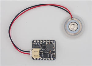
Programmable Mist Maker - XIAO / QT PY Extension
28 0 0 -
-
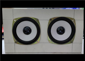
Bluetooth Speaker with Custom designed 15W dual channel Audio Amplifier
35 0 0 -
-
-
-
-
ARPS-2 – Arduino-Compatible Robot Project Shield for Arduino UNO
2701 0 5 -
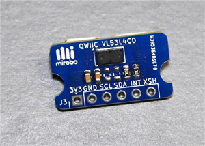
A Compact Charging Breakout Board For Waveshare ESP32-C3
3194 3 8