


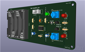
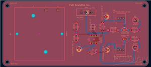
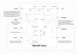

|
KiCADKicad
|
|
|
|
Microsoft ExcelMicrosoft
|
Breathing LED Circuit
Breathing LED Circuit
This dual-LED breathing circuit uses a classic NE555 timer in astable mode to smoothly alternate and fade a Red and Green LED without any microcontroller or code. By combining NPN and PNP transistor stages with RC charging networks and potentiometer controls, the circuit shapes a standard square-wave clock signal into breathing curves. Whether you are building this on a breadboard or walking through the accompanying mathematical model, this guide covers both the physical assembly and the underlying RC/transistor behavior that drives each fade cycle.
NE555N Pins:
- The inverter (-) on comparator 1 is connected to the non-inverter (+) on comparator 2. The trigger is connected to the threshold, causing the timer to flip-flop.
- When Pin 2 goes below 1/3 of Vcc, the comparator switches to high; when Pin 6 goes above 2/3 of Vcc, the comparator switches to high, resetting the flip-flop.
- Pin 7 discharges when Pin3 (Output) is low and Q̄ is high. When Q̄ is high, it turns on the base of the internal discharge transistor. The discharge pin is connected to the collector side of the transistor, which will discharge when the current in the base is sufficient.
- Pin 4 (Reset) is tied directly to the 6V rail to keep the timer active and prevent accidental resets.
- Pin 3 is the output.
- Pin 5 is used to eliminate Vcc noise with a bypass capacitor.
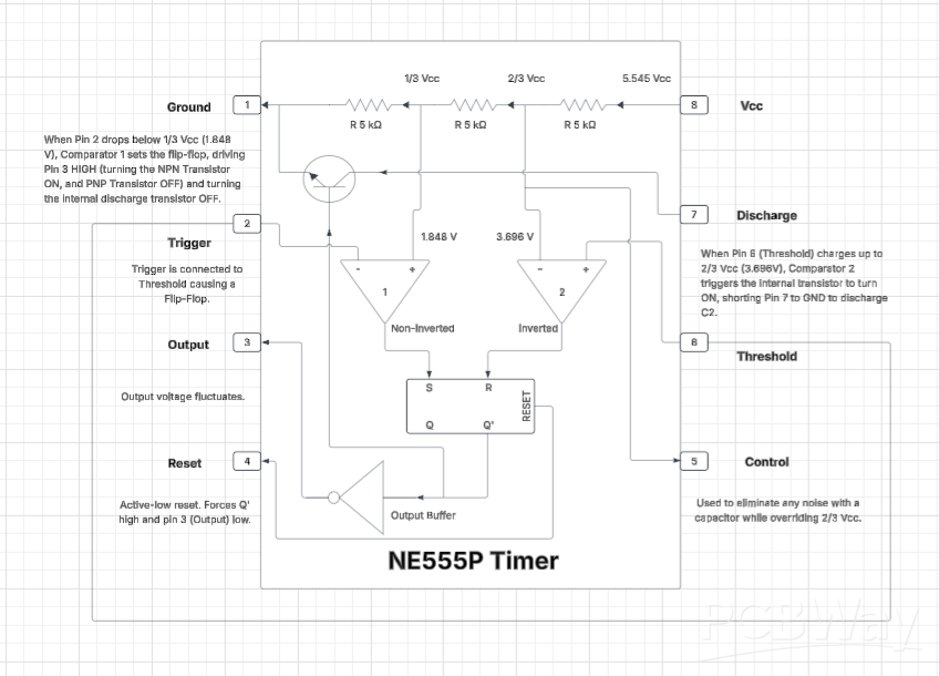
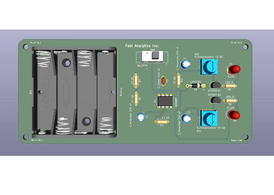
Figure 1
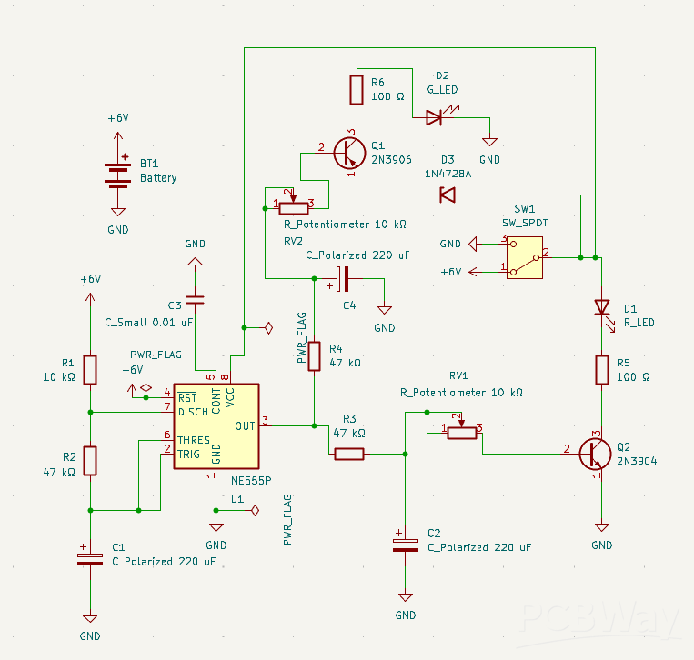
Figure 2
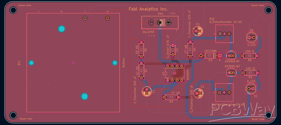
Figure 3
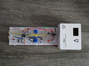
Breadboard/Prototype Instructions:
- Place the D3 in series with the 2nd pin of the switch and the Emitter of the PNP transistor. Make sure the cathode is connected to the emitter.
- Connect the 3rd pin of the switch to the GND rail.
- Connect the 1st pin of the switch to the Positive rail.
- Put R6 and the green LED in series with the collector terminal of the PNP transistor and GND.
- Connect the Base pin of the PNP transistor to the 3rd pin of the RV2.
- Connect pin 2 to pin 1 of the RV2.
- Connect pin 2 of RV2 to the anode of C4 and R4.
- Connect the cathode of C4 to the GND rail.
- Attach the other end of R4 to pin 3 of the timer.
- Connect R3 to pin 3.
- Connect the other end of R3 to the anode of C2 and pin 2 of RV1.
- Attach pin1 to pin 2 of RV1.
- Connect the 3rd pin of RV2 to the Base pin of the NPN transistor.
- Connect the Emitter pin of the NPN transistor to the GND rail.
- Connect the anode of the red LED to the second pin of the switch while placing the cathode in series with R5 and the Collector pin of the NPN transistor.
555 Timer connections:
- Connect the 2nd pin of the slide switch to pin 8 of the timer.
- Attach pin 4 to the positive rail.
- Connect pin 7 between R1and R2 to create a voltage divider.
- Place C3 in series with the GND rail and pin 5 of the timer.
- Attach pin 1 to the GND rail.
- Connect pin 6 to pin 2 to create the trigger/threshold subcircuit.
- Connect the anode of C1 to R2, pin 6 and pin 2 of the timer.
- Connect the cathode of C1 to the GND rail.
- Flip the slide switch to turn the LEDs ON.
- Slowly rotate the potentiometers to gradually adjust the timing of the capacitance of C2 and C4.
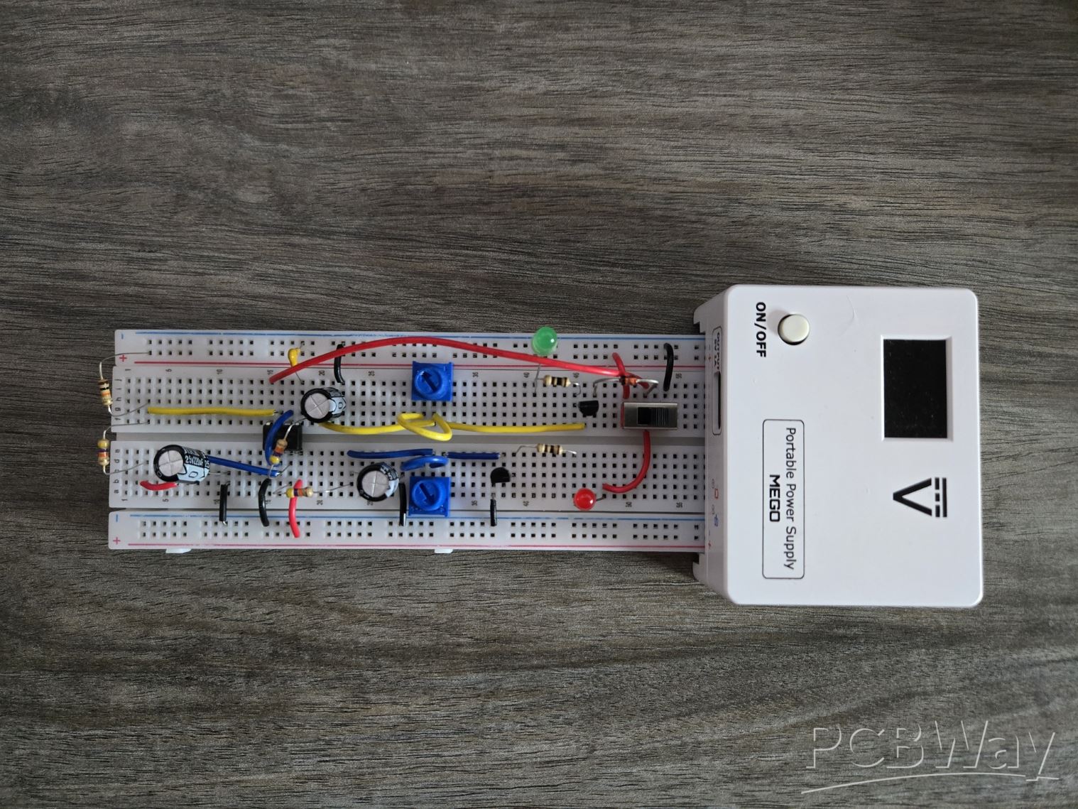
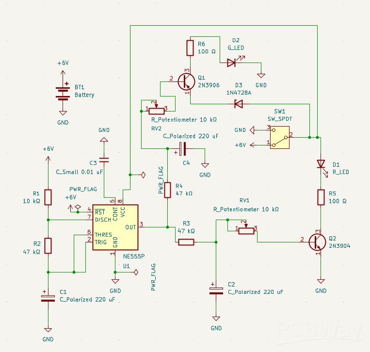
Figure 4
In addition to the prototype, I’ve attached a spreadsheet that calculates the voltage, current, and—most importantly—the RC timing of the capacitors. The resistor networks limit how fast current flows into and out of the electrolytic capacitors: higher resistance slows down the charge and discharge cycles, while lower resistance speeds them up.
The red LED is driven by an NPN transistor. It turns ON whenever there is at least 0.7 V at the base, allowing current to flow from the collector to the emitter. The PNP transistor driving the green LED works in the opposite way: when Pin 3 of the 555 timer is HIGH, the PNP base is reverse-biased and the green LED stays OFF. Once Pin 3 switches LOW, the PNP transistor turns ON and the green LED illuminates.
Because the PNP emitter is referenced to the positive supply rail rather than ground, the green LED branch operates at a higher voltage range than the red LED branch. Applying Kirchhoff’s Voltage Law (KVL) around the PNP base-emitter loop explains why: because current flows out of the PNP base toward Pin 3, the base-emitter voltage drop () adds directly on top of Pin 3’s 4.7 V HIGH output (). This sets the effective upper reference ceiling at 5.4 V in the charge formula. In addition, diode D3 drops the 6.0 V supply rail seen by the PNP emitter so the green LED can turn fully OFF when Pin 3 is HIGH—without D3, the difference between the 6.0 V rail and Pin 3's 4.7 V output would leave 1.3 V across the emitter-base junction, keeping the transistor partially ON.
Meanwhile, the main timing capacitor (C1) charges from the 6.0 V supply through the timing resistors while Pin 3 is HIGH, until reaching the upper threshold where Pin 7 switches to ground and discharges C1.
Breathing LED Circuit
Project images are for reference only. Actual production is based on the manufacturing files on the project page.
Please review the designer's notes (e.g., PCB thickness) and select the appropriate options.
PCBWay is not responsible
for issues caused by unsuitable parameter selections.
For more important ordering information, please refer to
Read More




Raspberry Pi 5 7 Inch Touch Screen IPS 1024x600 HD LCD HDMI-compatible Display for RPI 4B 3B+ OPI 5 AIDA64 PC Secondary Screen(Without Speaker)
BUY NOW


- Comments(0)
- Likes(0)
More by Preston Fabbi
-
-
-
-
-
-
-
AudioLink – USB & Bluetooth LE Audio / Auracast Receiver with Balanced Line Outputs (nRF5340)
449 0 1 -
-
-
-
Émetteur Récepteur Optique Expérimental (communication UART ATtiny + fibre optique)
453 0 1