Machine Learning Based GPS L1 Spoofing Detection System
GPS L1 Spoofing Detection System
Project Team
This project is carried out by a four-member Final Year Project group from the University of Moratuwa:
- Shenal Ranasinghe : likedin
- Kavishka Abeywardhana
- Pramidu Saumyajith
- Thathsara Dassanayaka
Academic Advisors:
- Dr. Sampath Perera
- Dr. Chamira Edussooriya
Department of Electronic and Telecommunication Engineering
University of Moratuwa, Sri Lanka
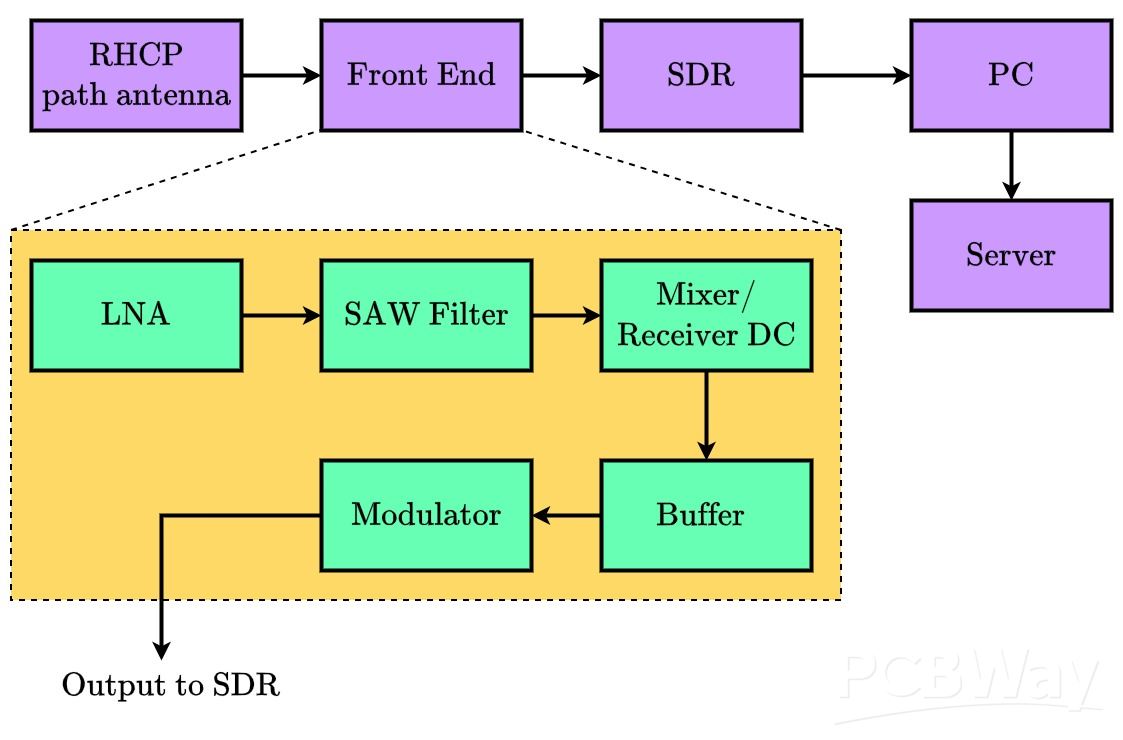
The machine learning architecture details are confidential at the moment as we are planning to publish a paper so this could affect the acceptance of that. therefore only the antenna -> RF PCB -> SDR is explained here
Project Overview
The Global Positioning System (GPS) is a satellite-based navigation system that provides precise positioning, navigation, and timing (PNT) information to a wide range of civilian and industrial applications, including transportation, telecommunications, power grids, autonomous systems, and scientific research. GPS signals are broadcast from satellites at very low power levels and are received on Earth below the thermal noise floor, making them inherently vulnerable to interference and malicious manipulation. GPS spoofing is a form of attack in which counterfeit navigation signals are transmitted to mislead a receiver into calculating incorrect position or time information while appearing authentic. Such attacks pose serious risks, as corrupted GPS data can disrupt navigation safety, desynchronize communication networks, degrade critical infrastructure timing, and undermine the reliability of GNSS-dependent systems. As reliance on GPS continues to grow, mitigating spoofing attacks has become increasingly important to ensure the integrity, availability, and trustworthiness of positioning and timing information. Effective mitigation requires not only advanced signal processing and detection algorithms, but also carefully designed RF front-end hardware capable of preserving signal fidelity, phase coherence, and noise performance, enabling reliable identification of anomalous or malicious signal behavior.
In this project, we aim to develop a GPS L1–band–targeted spoofing detection system that combines a carefully designed RF front-end PCB with machine learning–based analysis. The RF front end will be optimized to receive and condition weak GPS L1 signals at 1575.42 MHz while preserving key signal characteristics such as amplitude stability, phase continuity, spectral content, and noise behavior. The conditioned signals will be captured using a software-defined radio (SDR) platform and used to extract meaningful physical-layer features that reflect normal and anomalous GNSS signal behavior. These features will then be analyzed using data-driven machine learning techniques to distinguish authentic satellite signals from spoofed or manipulated signals. By focusing on the GPS L1 band and emphasizing high-fidelity RF signal acquisition, the system is designed to support controlled experimentation, repeatable validation, and extensibility to future GNSS security research, while keeping the RF hardware as a reusable and standalone research platform.
System Architecture
RF Front-End PCB Design & Prototyping
Project Overview
- We are a Final Year Project (FYP) group from the Department of Electronic and Telecommunication Engineering, University of Moratuwa, Sri Lanka, working on the development of a GPS L1 (1575.42 MHz) spoofing detection system, with a strong focus on RF front-end PCB design and validation.
- GNSS signals at the GPS L1 band are inherently extremely weak (below the thermal noise floor) and highly susceptible to interference and spoofing. As a result, the RF front-end PCB plays a critical role in preserving signal integrity, phase stability, and noise performance before any digital or algorithmic processing takes place.
- This project aims to develop a dedicated RF front-end PCB that serves as a high-fidelity, reusable hardware platform for GNSS signal integrity research and spoofing analysis.
Role of the RF Front-End PCB
The RF front-end PCB is the core hardware component of the system and is responsible for:
- Interfacing directly with an active/passive GPS L1 antenna
- Preserving extremely weak GNSS signals with minimal added noise
- Providing a controlled and repeatable RF interface to an SDR platform
- Enabling accurate experimentation and validation of spoofing scenarios
- The PCB is designed as a standalone RF module that bridges the analog RF domain and digital SDR-based processing.
RF PCB Architecture
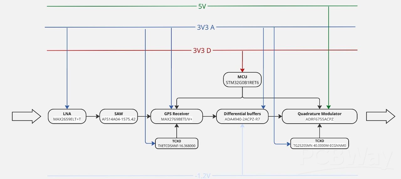
- The RF front-end PCB includes the following key stages:
- Antenna interface and impedance matching (50 Ω controlled impedance)
- Low-noise amplification (LNA) stage optimized for GPS L1
- Band-pass filtering centered at 1575.42 MHz to suppress out-of-band interference
- Signal buffering and isolation to prevent loading effects
- Frequency translation / conditioning for compatibility with SDR input requirements
- Carefully designed RF connectors and transitions (SMA / U.FL)
PCB Specifications
Layer Stackup
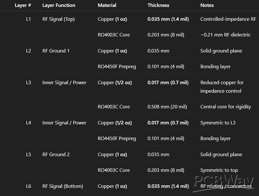
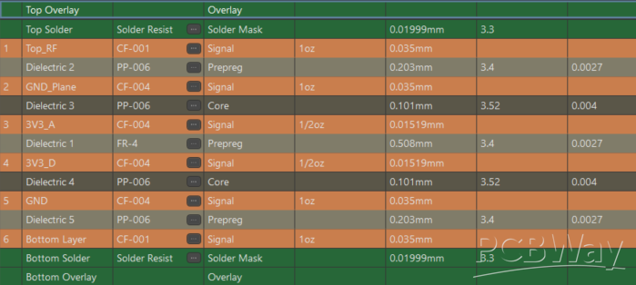
The RF front-end is implemented on a custom 6-layer PCB designed for GPS L1 (1575.42 MHz) operation. A Rogers high-frequency laminate is used instead of FR-4 to reduce dielectric loss and maintain stable impedance and phase performance at L-band. The board uses a custom layer stackup with dedicated RF signal layers referenced to continuous ground planes, along with internal power and shielding layers. This stackup enables controlled-impedance routing, low-noise operation, and effective RF isolation. A detailed image of the custom layer stackup is provided.
Special attention is given to:
- Controlled impedance microstrip routing
- Continuous RF ground planes
- Via stitching and grounding strategies
- EMI/EMC-aware component placement
- Minimization of phase distortion and insertion loss
- The PCB layout is treated as an RF structure, not just an interconnect, and is designed and verified using electromagnetic simulation tools.
- Simulation, Design, and Validation
Multiple PCB design iterations are required to achieve the desired RF performance. Each iteration involves:
- RF layout optimization
- Electromagnetic simulation (S-parameters, impedance, field behavior)
- Fabrication and measurement using SDR-based test setups
- Design refinement based on measured results
High-quality PCB fabrication is essential to ensure:
- Accurate impedance control
- Reliable RF performance at 1.575 GHz
- Repeatable and trustworthy measurement results
Use of PCBs in This Project
- PCBs are used extensively throughout the project to:
- Validate RF front-end design assumptions
- Compare multiple layout and filtering approaches
- Enable rapid design–test–iterate cycles
- Produce publishable, professional-grade RF hardware
- The RF front-end PCB developed in this project is not a one-off board, but a research platform that can support future GNSS-related studies beyond spoofing detection.
Why PCB Sponsorship Is Important
- As a student-led RF research project, access to professional PCB manufacturing is a major challenge. Support from PCBWay would allow us to:
- Rapidly prototype multiple RF PCB revisions
- Improve RF performance through iteration
- Gain hands-on experience in high-frequency PCB design
- Produce hardware suitable for academic publication and demonstrations
- PCBWay’s support would directly contribute to both the technical success of the project and the training of future RF engineers.
- Comments(0)
- Likes(1)