FPGA Based 5-Level Cascaded H-Bridge Single-Phase Inverter.
Comparison Evaluation of Various PWM Methods on an FPGA-Based 5-Level CHB Single-Phase Inverter.
Who we are
We are a team of four final-year Electrical and Electronics Engineering students from the Rajiv Gandhi Institute of Technology, Kerala, affiliated with APJ Abdul Kalam Technological University, India. Our passion for power electronics and embedded system has driven us to undertake this innovative project, where we aim to develop efficient and industry-relevant inverter technology.
Introduction
Pulse Width Modulation (PWM) techniques are the backbone of modern power electronics, shaping the quality of inverter output and determining overall efficiency. In Cascaded H-Bridge (CHB) inverters, PWM strategies directly influence Total Harmonic Distortion (THD), switching losses, and voltage utilization. This project takes a deep dive into three major PWM techniques—Sinusoidal PWM (SPWM), Multilevel Selective Harmonic Elimination PWM (MSHE-PWM), and Bus Clamping PWM (BCPWM)—comparing their performance on a 5-level CHB inverter controlled by an FPGA-based real-time system. The findings from this research project are intended for publication in IEEE and aims to advance FPGA-based inverter control methodologies.
Why PWM Matters in CHB Inverters?
Multilevel inverters are crucial for renewable energy integration, industrial motor drives, and grid-tied applications, but their performance is highly dependent on the PWM strategy used. The challenge lies in reducing harmonic distortion while optimizing switching efficiency—a balance that different PWM methods approach in unique ways.
- Sine-Triangle PWM (SPWM): is the simplest and most widely used PWM method. It works by comparing a sine wave with a high-frequency carrier triangle wave to generate switching signals. While easy to implement, it often results in higher switching losses.
- Multilevel Selective Harmonic Elimination PWM (MSHE-PWM): goes a step further, leveraging Fourier analysis to calculate precise switching angles that eliminate specific lower-order harmonics (3rd, 5th, 7th, 9th, 11th). This results in reduced THD and switching losses, making it an attractive option for high-power applications. However, the complex computational task makes it challenging for online load regulation.
- Bus Clamping PWM (BCPWM): introduces an innovative approach by minimizing inverter switching losses while maintaining a reasonable THD level. Instead of switching continuously between states, it "clamps" the bus voltage to reduce transitions—resulting in better efficiency without significantly affecting harmonic content.
Hardware Implementation: FPGA at the Core
To achieve real-time performance, the inverter is controlled by a custom-designed Spartan-7 FPGA board, allowing ultra-fast switching signal generation and online load adaptation. Unlike traditional microcontrollers, the FPGA processes multiple control algorithms in parallel, ensuring that the inverter responds dynamically to load variations while optimizing power conversion.
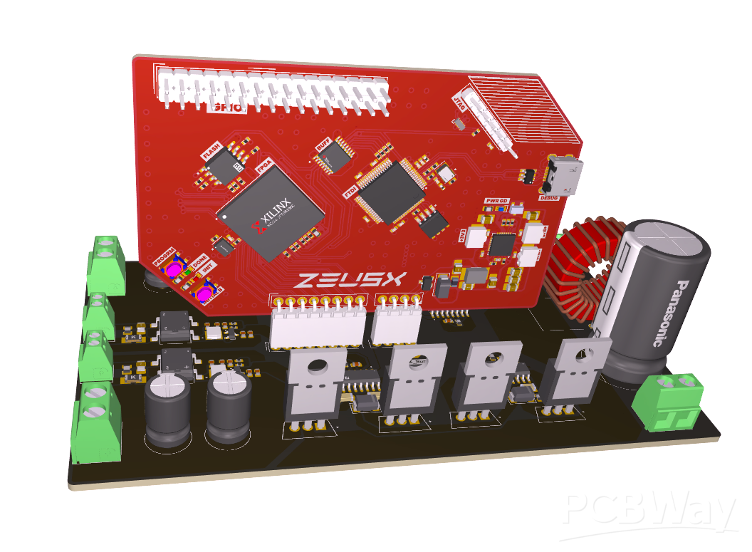
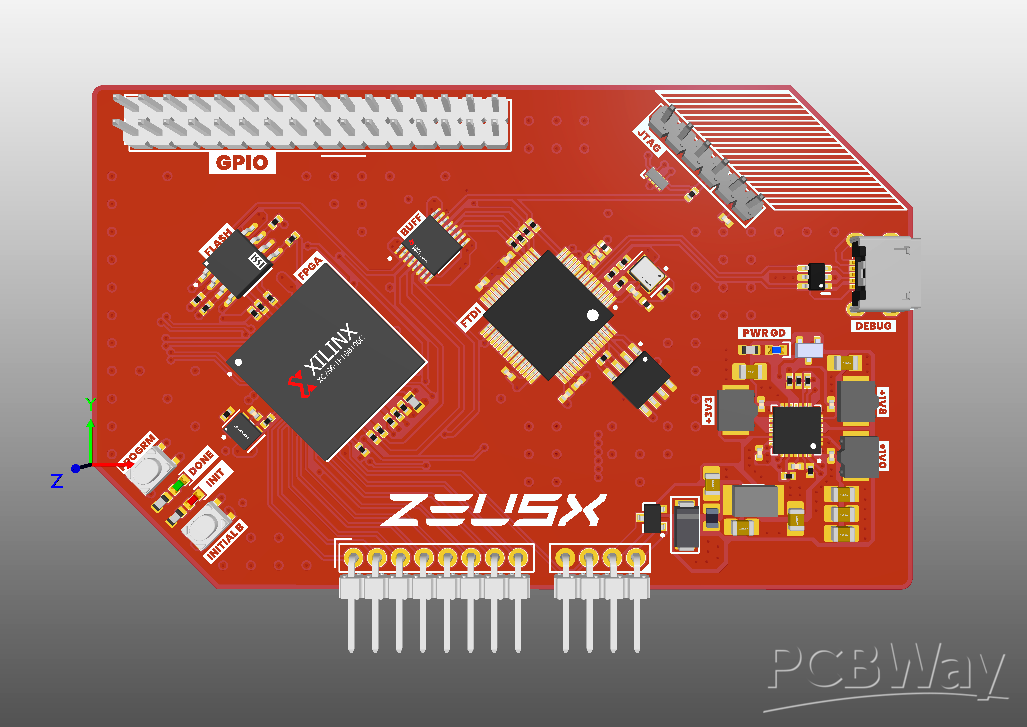
FPGA Development Board (ZeusX):
- Core: Spartan-7 FPGA (XC7S6-1FTGB196C)
- Memory: 64MB QSPI flash for rapid configuration
- Debugger: FTDI FT2232H USB-to-JTAG
- Power: Quad buck converter MAX20029ATIF/V+
- Design: 4-layer PCB for robust signal integrity
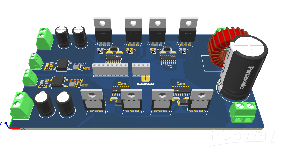
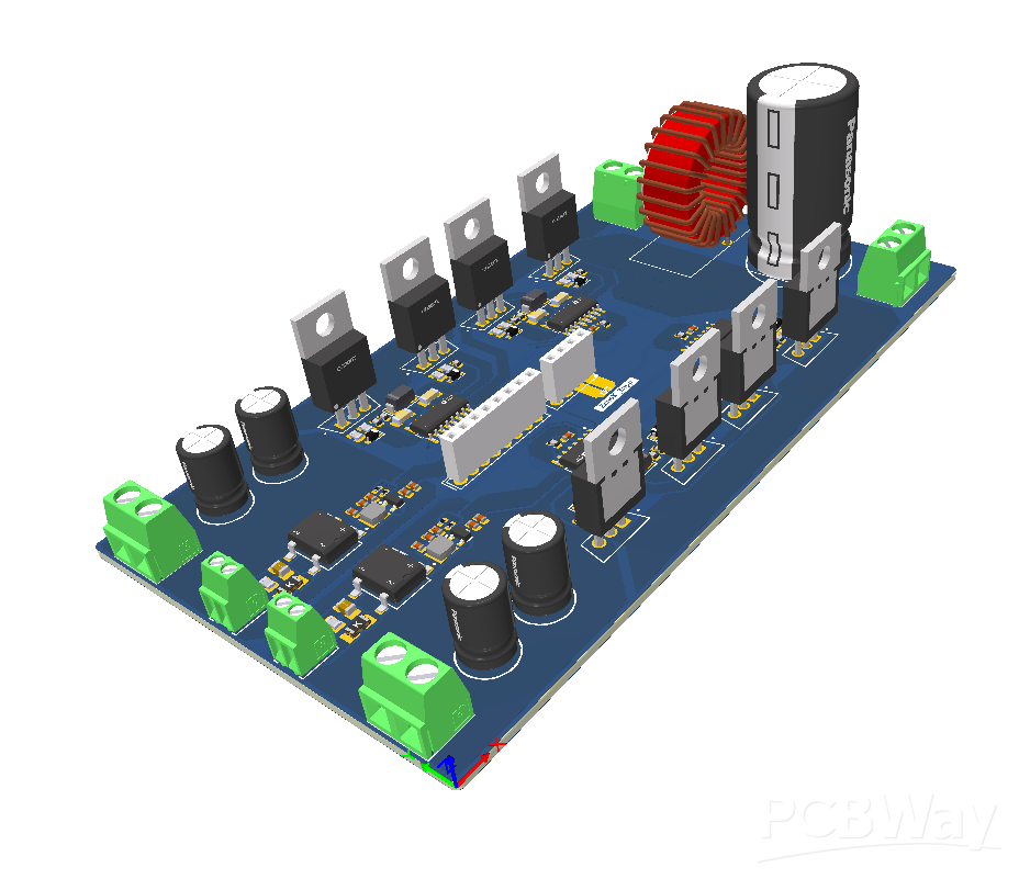
Inverter Board:
- Size: 130 x 80 mm, 2-layer PCB
- MOSFETs: 8 nos (STF16N60M2, Vds max = 600V, Id = 12A)
- Gate Driver: ADDUM3223 dual-channel isolated gate driver
- Filtering: LC filter for cleaner output
Simulation & Real-World Testing
Before hardware implementation, the inverter was simulated using MATLAB/Simulink, where FFT analysis was performed to measure harmonic distortion across different PWM techniques. The hardware verification was later performed using the WAVECT WCU300 module for real-time validation, ensuring the validity of the final inverter module design. The final step of the project is the PCB manufacturing process.
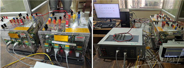
Fig: Hardware verification using WAVECT WCU300 module.
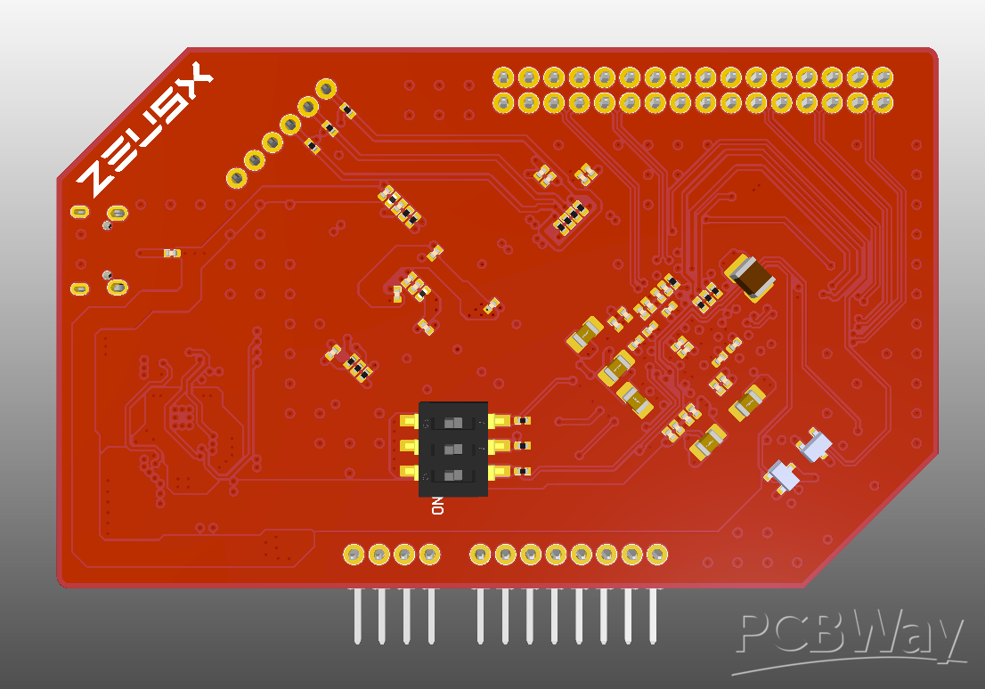
The final PCB design:

Words to PCBWay
The implementation of our FPGA-Based 5-Level Cascaded H-Bridge Inverter involves significant financial investment, particularly in the manufacturing and assembly of custom PCBs. The FPGA development board (ZeusX), being a complex 4-layer design including BGA & QFN packages, incurs a substantial production cost, making it a critical component in need of sponsorship. This project has the potential to advance power electronics, enhance inverter efficiency, and contribute to renewable energy integration, impacting industries such as solar power, industrial motor drives, and smart grid systems. PCBWay's support in the form of PCB manufacturing and assembly sponsorship, ideally for both boards, or at the very least, for the FPGA development board, would help us realize this innovation and drive meaningful progress in the field. We look forward to the possibility of collaborating with PCBWay to bring this project to life.
Apply for sponsorship >>- Comments(0)
- Likes(0)