

DIY USB-C Power Bank PCB
The move towards USB-C is a great thing to bring a universal connector to all devices, making life more convenient. Unfortunately, power banks until now have been slow to make the move, sticking to USB-A and Micro usb. I designed a custom PCB which provides both USB-C Charging but also USB-C output for up to 22.5W, and it still features a USB-A port for backwards compatibility. The circuit itself is designed for 10,000mAh but can be configured for other capacities. I made it open source on GitHub to help others to learn as well. The circuit uses the IP5358-BZ, an IC which supports USB-C, battery protection for over/underdischarge as well as over/under voltage/current. Whilst my implementation is largely based on the provided data sheet, it is in Chinese so I had to rely on google translate to understand it. If you feel any improvements can be made to the circuit or that I am missing anything, please comment below. All feedback is appreciated.
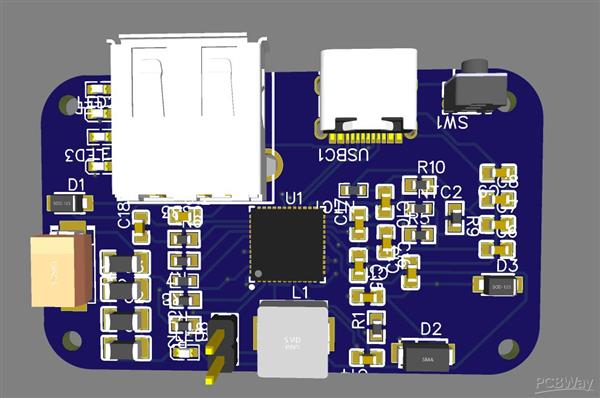
This is the schematic of the project. The IC supports bi-directional USB-C which can be implemented quite easily. Thanks to the built in CC1 and CC2 resistor management, the IC is able to switch between power input and output, which is very valuable when saving space and cost of components on the PCB. As explained earlier, a much simpler implementation of a USB-A port was also included for compatibility with older products which are still stuck with USB-C. Whilst the IC can support micro-usb, I intentionally steered away from it since the entire reason behind this project was to move away from old standards and embrace, new universal ones. Functionally, the IC also support battery management and charge detection/percentage. This was implemented via 4 LEDs to display how much it was charged. LED 5 exists to indicate whether the power bank is successfully charging via the Output. The PCB below show cases the ideal lay for which I will later design a 3D Printable case. Whilst the routing below is only preliminary and is frankly a mess right now, I hope to improve it at a later stage before fabrication by optimising spacing between components and maximising trace widths. The biggest concern I have right now is the circuits ability to hope with high currents as well as possible issues with EMI. I have to ensure correct grounding, and the instructional videos from Altium have been incredibly educational so far in helping me understand how to do this correctly.
About me:
I am a 15 year old student looking to explore PCB design by working on DIY projects to help me learn more about circuit design and the work that actually goes behind it. Unfortunately I have a limited budget and do not have the tools to solder components myself so I am basically relying on the possibility of a sponsorship to make this reality!
Apply for sponsorship >>- Comments(1)
- Likes(4)
 More by Muhammad Shah
-
 Minimal P1P Enclosure
I plan to create an affordable enclosure for the P1P which can allow beginners to get into 3D printi...
Minimal P1P Enclosure
I plan to create an affordable enclosure for the P1P which can allow beginners to get into 3D printi...
-
 DIY 40% Keyboard: A budget perspective.
This project aims to introduce students to the world of PCB design by providing a tangible and funct...
DIY 40% Keyboard: A budget perspective.
This project aims to introduce students to the world of PCB design by providing a tangible and funct...
-
 DIY USB-C Power Bank PCB
The move towards USB-C is a great thing to bring a universal connector to all devices, making life m...
DIY USB-C Power Bank PCB
The move towards USB-C is a great thing to bring a universal connector to all devices, making life m...