Disclaimer: This circuit is an industrial upgrade for the capacitor-based supply solution, it is connected to the 220V-AC Mains, non-galvanically isolated. if you are not familiar with the electrical safety rules, please avoid this content or ask some professionals to guide you. The author (or anybody else or any company) is NOT responsible for any harm or damage. Do it at your own risk. This is not for beginners!
By Hesam Moshiri, Anson Bao
Whenever you hear the transformerless supply term, you initially imagine the capacitor-based solution, which means a high voltage capacitor in series with the mains line, then a bridge rectifier, a Zener diode, a filtering capacitor, and so on. Such a circuit is not just unable to deliver sufficient current for many applications, also, it is not a reliable solution for the industry, although you might see such circuits in some cheap products that are designed to have a low cost.
A month ago, I was repairing a washing machine mainboard. In the examination process, I realized that it is equipped with an LNK304 chip that is used in transformerless supplies. So I decided to design a circuit based on this chip to be used in your applications. The circuit contains 220VAC mains input protection, output filtering, and a regulator.
To design the schematic and PCB, I used Altium Designer 22 and the SamacSys component libraries (Altium plugin). To get high-quality fabricated PCB boards, I sent the Gerbers to PCBWay and purchased original components using the componentsearchengine.com. To test the current handling and stability of the output voltage, I used the Siglent SDL1020X-E DC Load and examined the power supply output noise using the Siglent SDS2102X Plus oscilloscope.
Specifications
Input Voltage: 220VAC+/-15%
Output Voltage: 5VDC
Output Current (Continous): 120mA to 150mA (can be increased, see text)
Output Current (Short time): 180mA
Output Noise (max): 30mVp-p (150mA load, 20MHz BW)
Input Protection: Fuse, NTC, Varistor
Output protection: short circuit and current limit at around 190mA
• Download the Gerbers, or order 10Pcs high-quality boards, for just 5USD
• To order a fully assembled PCB board (Plus FREE shipping). Please contact: anson@pcbway.com
Circuit Analysis
Figure 1 shows the schematic diagram of the device. As it is clear, the circuit contains three main parts: the 220V Mains input circuit, LNK304, output filtering, and a 5V regulator.
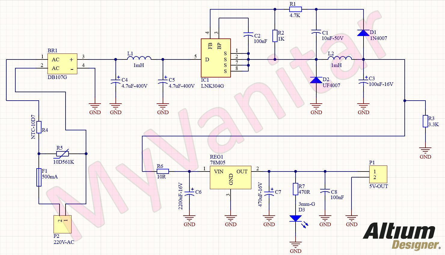
Figure 1
Schematic diagram of the transformerless power supply using LNK304
220VAC Mains Input
The Mains input protection consists of F1, R4, and R5. R5 is the 10D561 Varistor. According to the datasheet: “Varistors are voltage-dependent, a nonlinear device which has an electrical behavior similar to back-to-back Zener diodes. TYEE series zinc oxide varistors are nonlinear resistors, consisting main of zinc oxide and several kinds of metal oxide additives. They are bilateral and symmetrical V-I characteristics curve and unparalleled large peak current capability are used for absorption of transient voltage, suppression of pulse noise and circuit voltage stabilization.”
We are not sure where this circuit is gonna be used. So we have to protect it against switching surges from various kinds of relays and electromagnetic valves using a varistor like the abovementioned one.
F1 is an ordinary 500mA fuse that naturally protects the circuit against any weird incidents that might cause huge current leakage, explosion, or even fire. R4 is the 10D7 NTC that protects the circuit against inrush currents. BR1 is the DB107G bridge rectifier [1] and C4, C5, and L1 build a low pass Pi filter to reduce the noise and ripple as much as possible.
LNK304
The main component of this circuit is IC1, LNK304 indeed [2]. According to the datasheet: “LinkSwitch-TN is specifically designed to replace all linear and capacitor-fed (cap dropper) non-isolated power supplies in the under 360 mA output current range at equal system cost while offering much higher performance and energy efficiency. LinkSwitch-TN devices integrate a 700 V power MOSFET, oscillator, simple On/Off control scheme, a high-voltage switched current source, frequency jittering, cycle-by-cycle current limit, and thermal shutdown circuitry onto a monolithic IC. The start-up and operating power are derived directly from the voltage on the DRAIN pin, eliminating the need for a bias supply and associated circuitry in a buck or flyback converters. The fully integrated auto-restart circuit in the LNK304-306 safely limits output power during fault conditions such as short-circuit or open loop, reducing component count and system-level load protection cost. A local supply provided by the IC allows the use of a non safety graded optocoupler acting as a level shifter to further enhance line and load regulation performance in buck and buck-boost converters if required.”
R1 and R2 define the output voltage of the chip. C1, C2, C3, L2, D1, and D2 are selected according to the datasheet. R3 creates a preliminary light load to stabilize the output voltage.
Output Filter and Regulator
R6 and C6 create a low-pass RC filter to reduce the output noise and ripple. REG1 is the 78M05 regulator [3] to build a stable +5V output. The +5V level is a norm for many applications (such as powering an Arduino board and accessories), so I decided to use a +5V regulator. If your load requires a +3.3V voltage rail, simply use another regulator (an LDO type preferably) just near the load. The voltage level before R6 is around 9.5V, so by 150mA current consumption, this filter introduces a 1.5V voltage drop, however, 8V is still an acceptable input voltage for the REG1 to handle a stable +5V at the output.
C7 is the output stabilizer capacitor for the regulator and D3 LED indicates that there is a proper voltage at the output. R7 limits the current to D3 and C8 helps to remove high-frequency noises even further.
PCB layout
Figure 2 shows the PCB layout of the design. It’s a two layers PCB board and the majority of the components are through-hole.

Figure 2
PCB layout of the transformerless power supply using LNK304 (Altium)
When I decided to design the schematic and PCB for this project, I realized that I don’t have the component libraries of BR1[4], IC1[5], and REG1[6] in my component libraries storage. So as usual, I selected IPC-rated SamacSys component libraries and installed the missing libraries (schematic symbol, PCB footprint, 3D model) using the free SamacSys tools and services. There are two ways to import the libraries: You can visit the componentsearchengine.com and download and import the libraries manually, or you can use the SamacSys CAD plugins and automatically import/install the libraries into the design environment. Figure 3 shows all supported electronic designing CAD software [7]. As it is clear, all famous players are supported. I use Altium Designer, so I installed the missing libraries using the SamacSys Altium plugin (Figure 4) [8]. Figure 5 shows a 3D view of the PCB board and assembly drawings.

Figure 3
All supported electronic designing CAD software by the SamacSys plugins

Figure 4
Selected component libraries in the SamacSys Altium plugin

Figure 5
A 3D view and two assembly drawings of the PCB board
Assembly and Test
Figure 6 shows the assembled PCB board. The input connector (220V AC) is firm enough to provide a good and stable connection for the 220V Mains. The output connector is a 2.5mm XH male connector.

Figure 6
Assembled PCB board of the transformerless power supply
I used the Siglent SDL1020X-E DC Load [9] to test the output for current handling and voltage stability. Figure 7 shows a part of the experiment. I configured the DC load to CC (constant current) and increased the current till the output voltage turns OFF. The result is the point of the current limit threshold. To test the continuous current handling, I adjusted the DC Load to 150mA of continuous current and tested the board for around an hour. This experiment handles the continuous current point, at room temperature. You might be able to reach a higher current, however, you have to reduce the temperature using a heatsink or a FAN. Please watch the YouTube video for more details.

Figure 7
Testing the supply output for current handling and voltage stability, using the Siglent SDL1020X-E
To test and examine the output noise, I used the Siglent SDS2102X Plus oscilloscope [10]. It’s a cute piece of equipment with a 10-inch touch display. I put the DC Load on 150mA of current and examined the supply noise in the peak detect acquisition mode and a ground spring on the probe tip. Figure 8 shows the output noise. Please watch the YouTube video for more details.

Figure 8
Testing the power supply output for noise, using the Siglent SDS2102X Plus oscilloscope
Future Work
I used an RC filter (R6, C6) to reduce the noise. You can try to use an LC filter, however, be careful about the cut-off frequency of the filter, frequency of the noise, and oscillation [11].
You can achieve a higher output current by using the LNK305 or LNK306 chips. In the case of using an LNK306 chip, the output current can reach 350mA. So you have to reduce the R6 value or use an LC filter with the pre-mentioned consideration. Also, mount a small heatsink on the output regulator.
Bill of materials
Figure 9 shows the bill of materials and part numbers for this project.

Figure 9
Bill of materials for the transformerless power supply using LNK304
References
[1]: DB107G datasheet: https://datasheet.datasheetarchive.com/originals/distributors/Datasheets-DGA18/326891.pdf
[2]: LNK304G datasheet: https://eu.mouser.com/datasheet/2/328/lnk302_304-306-1512550.pdf
[3]: 78M05 datasheet: https://www.onsemi.com/pdf/datasheet/mc78m00-d.pdf
[4]: DB107G schematic symbol, PCB footprint, 3D model: https://componentsearchengine.com/part-view/DB107-G/Comchip%20Technology
[5]: LNK304G schematic symbol, PCB footprint, 3D model: https://componentsearchengine.com/part-view/LNK304GN-TL/Power%20Integrations
[6]: 78M05 schematic symbol, PCB footprint, 3D model: https://componentsearchengine.com/part-view/MC78M05CDTG/onsemi
[7]: Electronic designing CAD software plugins: https://www.samacsys.com/library-loader-help
[8]: Altium Designer plugin: https://www.samacsys.com/altium-designer-library-instructions
[9]: Siglent SDL1020X-E DC load: https://siglentna.com/dc-electronic-load/sdl1000x/
[10]: Siglent SDS2102X Plus oscilloscope: https://www.siglenteu.com/digital-oscilloscopes/sds2000xp/
[11]: Output Noise Filtering for DC/DC Power Modules, Application Report, SNVA871–April 2019: https://www.ti.com/lit/an/snva871/snva871.pdf?ts=1651054084433&ref_url=https%253A%252F%252Fwww.google.com%252F


