In this step-by-step tutorial you’ll learn how to design your own custom microcontroller board based on the popular STM32 microcontroller from ST Microelectronics

Written by John Teel
I’ll break down the entire design process into three fundamental steps:
When developing a new circuit design the first step is the high-level system design (which I also call a preliminary design). Before getting into the details of the full schematic circuit design it’s always best to first focus on the big picture of the full system.
Designing the system consists mainly of two steps: creating a block diagram and selecting all of the critical components (microchips, sensors, displays, etc.). A system design treats each function as a black box
In engineering, a black box is an object which can be viewed in terms of its inputs and outputs but without any knowledge of its internal workings. With a system-level design the focus is on the higher level interconnectivity and functionality.
Below is the block diagram that we’ll be working from in this tutorial series. As I mentioned, for this first tutorial we’ll focus just on the microcontroller itself. In future tutorials we’ll expand the design to include all of the functionality shown in this block diagram.
A block diagram should include a block for each core function, the interconnections between the various blocks, specified communication protocols, and any known voltage levels (input supply voltage, battery voltage, etc.).
Later, once all of the components have been selected and the required supply voltages are known I like to add the supply voltages to the block diagram. Including the supply voltage for each functional block it allows you to easily identify all of the supply voltages you’ll need as well as any level shifters.
In most cases when two electronic components communicate they need to use the same supply voltage. If they are supplied from different voltages then you’ll usually need to add in a level shifter.
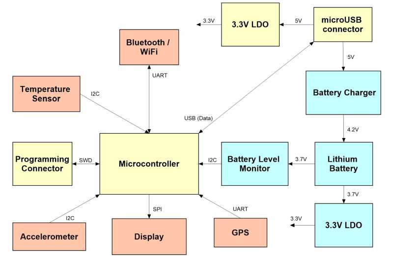
System-level block diagram. Blocks in yellow are included in this initial tutorial.
Now that we have a block diagram we can better understand the necessary requirements for the microcontroller. Until you’ve mapped out everything that will connect to the microcontroller it’s impossible to select the appropriate microcontroller.
When selecting a microcontroller (or just about any electronic component) I like to use an electronics distributor’s website like Newark.com. Doing so allows you to easily compare various options based on a variety of specifications, pricing, and availability. It’s also an easy way to quickly access the component’s datasheet.
If you regularly read this blog you’ll know that I’m a big fan of ARM Cortex-M microcontrollers. Arm Cortex-M microcontrollers are easily the most popular line of microcontrollers used in commercial electronic products. They have been used in tens of billions of devices.
Microcontrollers from Microchip (including Atmel) may dominate the maker market but Arm dominates the commercial product market.
Arm doesn’t actually manufacture the chips directly themselves. They instead design processor architectures that are then licensed and manufactured by other chip makers including ST, NXP, Microchip, Texas Instruments, Silicon Labs, Cypress, and Nordic.
The ARM Cortex-M is a 32-bit architecture that is fantastic choice for more computationally intensive tasks compared to what is available from older 8 bit microcontrollers such as the 8051, PIC, and AVR cores.
Arm microcontrollers come in various performance levels including the Cortex-M0, M0+, M1, M3, M4, and M7. Some versions are available with a Floating Point Unit (FPU) and are designated with an F in the model number such as the Cortex-M4F.
One of the biggest advantages of Arm Cortex-M processors is their low price for the level of performance you get. In fact, even if an 8-bit microcontroller is sufficient for your application you should still consider a 32-bit Cortex-M microcontroller.
There are Cortex-M microcontrollers available with very comparable pricing to some of the older 8-bit chips. Basing your design on a 32-bit microcontroller gives you more room to grow should you want to add additional features in the future.
The STM32 from ST Microelectronics is my favorite line of ARM Cortex-M microcontrollers.
Although numerous chip makers offer Cortex-M microcontrollers, my favorite by far is the STM32 series from ST Microelectronics. The STM32 line of microcontrollers is quite expansive with just about any feature and level of performance you would ever need. The STM32 line can be broken down into several subseries as shown in Table 1 below.

The STM32F subseries is their standard line of microcontrollers (versus the STM32L subseries which is specifically focused on lower power consumption). The STM32F0 has the lowest price but also the lowest performance. One step up in performance is the F1 subseries, followed by the F3, F2, F4, F7, and finally the H7.
For this tutorial I have selected the STM32F042K6T7 which comes in a 32-pin LQFP leaded package. I selected a leaded package primarily because it simplifies the debugging process because you have easy access to the microcontroller pins. Whereas with a leadless package, like a QFN, the pins are hidden away underneath the package making access impossible without test points.
A leaded package also allows you to more easily swap out the microcontroller if it were to become damaged. Finally, leadless packages cost more to solder on to the PCB so they increase both the prototyping and manufacturing costs.
I selected the STM32F042 because it offers moderate performance, a good number of GPIO pins, and various serial protocols including UART, I2C, SPI and USB. This is a fairly entry-level STM32 microcontroller with only 32 pins, but with a wide variety of features. More advanced versions come with as many as 216 pins which would be quite overwhelming for an introductory tutorial.
In this first video we won’t be using most of these features, but we will take advantage of them in future videos in this series.
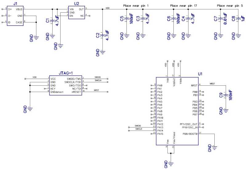
Schematic circuit diagram for this first tutorial showing the STM32 microcontroller, linear regulator, USB connector, and programming connector.
Now that we have selected the microcontroller it’s time to design the schematic circuit diagram. For these tutorials I’ll be using a PCB design tool called DipTrace.
There are dozens of PCB tools available but when it comes to ease of use, price, and performance I find that DipTrace is hard to beat, especially for startups and makers.
If you don’t have a PCB design package then you may want to consider downloading the free version of DipTrace so you can follow along closely with this tutorial. They also offer a free trial of their full version. The best way to learn something is always to actually do it.
For this initial tutorial the free version of DipTrace is sufficient, but for most designs you’ll need to upgrade to a paid version.
Nonetheless, this tutorial will be focusing on the process for designing a custom microcontroller board, and not on how to use any specific PCB design tool. So regardless of which PCB software you end up using you’ll still find these tutorials are just as useful.
The first step in designing a schematic is to place all of the key components. For this initial design this includes the microcontroller chip, a voltage regulator, a microUSB connector, and a programming connector.
For more complex designs it usually makes more sense to completely design each sub-circuit first, then merge them all together. Depending on the design complexity (and personal preference) you may also want to place each sub-circuit on its own separate sheet. This keeps the schematic from becoming a huge, overwhelming monster on a single sheet.
Next, we’ll place all of the various capacitors. For the most part you can think of capacitors as tiny little rechargeable batteries that hold electrical charge and help to stabilize the voltage on a supply line.
We’ll start by placing a 4.7uF capacitor on the input pin of the linear regulator. This is the 5VDC input voltage supplied by an external USB charger. This voltage is fed into a TLV70233 linear regulator which steps the voltage down to 3.3V since the microcontroller can only be supplied by a maximum of 3.6V.
Another 4.7uF capacitor is placed on the output of the regulator as close to the pin as possible. This capacitor serves to store charge to supply transient loads and it acts to stabilize the internal feedback loop of the regulator. Without an output capacitor most regulators will begin to oscillate.
Decoupling capacitors must be placed as close as possible to the microcontroller supply pins (VDD). It’s always best to refer to the microcontroller datasheet in regards to their recommendations for decoupling capacitors.
The datasheet for the STM32F042 recommends a 4.7uF and a 100nF capacitor be placed next to each of the two VDD pins (input supply pins). It also recommends 1uF and 10nF decoupling capacitors be placed near the VDDA pin.
The VDDA pin is the supply for the internal analog-to-digital (ADC) converter and must be especially clean and stable. We’re not using the ADC in this first tutorial but we will in a future one.
Note that you’ll commonly see two capacitor sizes specified together for decoupling purposes. For example, 4.7uF and 100nF capacitors.
The larger 4.7uF can store more charge which helps stabilize the voltage when large spikes in load current are required. The smaller capacitor serves mainly to filter out any high-frequency noise.
Although the STM32F042 offers a wide variety of functions such as UART, I2C, SPI, and USB communication interfaces, you won’t find any of these functions labeled on the microcontroller pinout. This is because most microcontrollers assign a variety of functions to each pin so as to reduce the number of pins required.
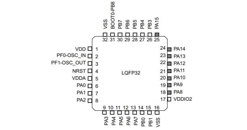
Pinout for the STM32F042 microcontroller in a 32-pin LQFP leaded package.
For example, on the STM32F042 pin 9 is labeled as PA3 which means it is a GPIO pin. Upon startup this function is automatically assigned to this pin. But it also has alternative functions that can be specified in the firmware program.
Pin 9 can be programmed to serve the following functions: receive input pin for UART serial communication, an input to the Analog-to-Digital Converter (ADC), a timer output, or an I/O pin for the capacitive touch sensor controller.
Refer to the pin definition table in the microcontroller datasheet (page 33 for the STM32F042) which shows all of the various functions available for each pin. Always be sure to confirm that two functions required for your product don’t overlap on the same pins.
All microcontrollers require a clock for timing purposes. This clock is just an accurate oscillator. Microcontrollers execute programmed commands sequentially with each tick of the clock.
The simplest option, if available on the selected microcontroller, is to use the internal clock. This internal clock is known as an RC oscillator clock because it uses the timing characteristics of a resistor and capacitor.
The major downside to an RC oscillator is accuracy. Resistors and capacitors (especially those embedded inside a microchip) vary significantly from unit to unit causing the oscillator frequency to vary. Temperature also significantly impacts the accuracy.
An RC oscillator is fine for simple applications, but if your application requires accurate timing then it won’t be sufficient. For this initial tutorial we’re going to use the internal RC clock to keep things simple. In future tutorials we’ll improve the design by adding a much more precise, external crystal-based oscillator.
Programming an STM32 is done via one of two protocols: JTAG or Serial Wire Debug (SWD). More advanced versions of the STM32 (STM32F1 and higher) offer both JTAG and SWD programming interfaces. The STM32F0 subseries offers only the simpler SWD programming interface so that is what we will focus on for this tutorial.
The SWD interface requires only 5 pins. They are SWDIO (data input/output), SWCLK (clock signal), NRST (reset signal), VDD (supply voltage) and ground.
Unfortunately the ST-LINK programmer device that you’ll use to program the STM32 uses a 20-pin JTAG connector (with SWD functionality). This connector is quite large and is not practical for smaller board designs.
Instead, you can use a 20-pin to 10-pin adapter board such as this one from Adafruit so you can use a smaller 10-pin connector on your board.
For this tutorial we will use the 10-pin connector. If that is still too large for your project then you can always use a 5-pin header and jumper wires from the 20-pin programmer output to connect only the 5 lines required for SWD programming.
The last part of the schematic we’ll cover is the power section. The STM32 microcontroller can be powered with a supply voltage from 2.0 to 3.6V. Unless you have a variable power supply, you’ll need an on-board regulator to provide the appropriate supply voltage.
For this design we’ll power the board using an external USB charger which outputs 5 VDC. This voltage will then feed into a linear voltage regulator (TLV70233 from Texas Instruments) which steps it down to a stable 3.3V.
The STM32 requires a maximum of only 24mA assuming none of the GPIO pins are sourcing any current (each GPIO pin can source up to 25mA). The absolute maximum current the STM32 will ever require is 120mA assuming various GPIO pins are sourcing current.
The TLV70233 is rated for up to 300mA which should be more than sufficient for this initial design. In future tutorials, as we add additional functions, we may need to revisit this to ensure the regulator can handle the required system current.
Electrical Rules Check
The final step of designing the schematic circuit diagram is to perform a verification step called an Electrical Rules Check (ERC). This verification step checks for errors such as shorts between nets, nets with only one pin, superimposed pins, and unconnected pins.
You can also setup various pin type errors. For example, if an output pin is connected to another output you will get an error. Or if an output pin is connected to a power supply line you will get an error. DipTrace uses a colored grid matrix that allows you to define which pin type connections will give you errors or warnings.
Once the schematic design is completed, it’s time to design the Printed Circuit Board. Begin by inserting all of the components into the PCB layout. In DipTrace, you can use the “Convert to PCB” function in the schematic to automatically create the PCB with all of the components inserted.
Although all of the components have been inserted, it’s your job to determine exactly where each component is placed on the PCB.
Most PCB design software packages include an auto-placement feature that places components with the goal of minimizing routing lengths. But I never use it, and it’s almost necessary to manually place the components in the best layout.
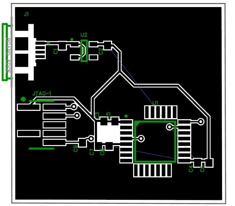
For our initial tutorial circuit, the component placement is pretty simple. Place the microUSB connector next to the linear regulator with its output as close as possible to the input supply pins (VDD) on the microcontroller. Finally, place the programming connector anywhere that is convenient.
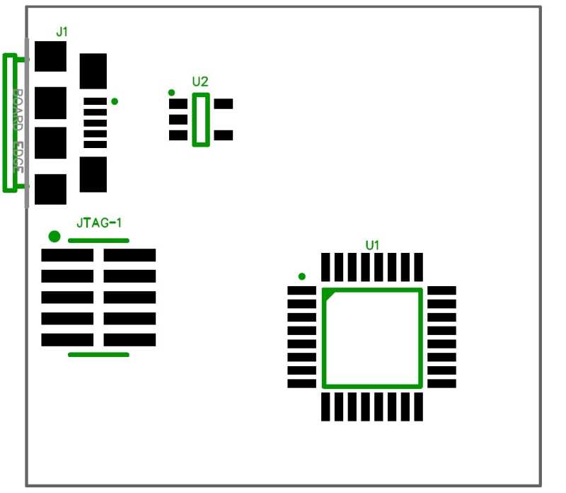
Placement of the critical components in this initial design: the microcontroller (U1), the regulator (U2), the micro USB connector (J1), and the programming connector (JTAG-1).
Once all of the core components are properly placed, your next step is placing all of the passive components (resistors, capacitors, and inductors). For this initial design the only passive components are capacitors.
One key aspect of designing electronics that you need to learn is the concept of parasitics. Parasitics are passive components (resistors, capacitors, and inductors) that you don’t intentionally design into your circuit. But, nonetheless, they are there and impact performance.
For example, although a signal trace is intended to be a perfect short, it in fact has some finite resistance, capacitance, and inductance all of which become more significant as the trace length increases, and as the number of bends and vias increase.
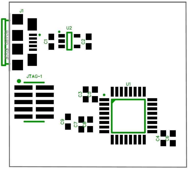
Placement of all critical components (U1, U2, J1, and JTAG-1) and the passive components (capacitors).
So this means that if a voltage source is located far away from the load, which is the STM32 microcontroller in this case, there is essentially a resistor between the load and the source (neglecting any capacitance and inductance).
If the microcontroller all of a sudden requires a fast spike of current then it will cause a voltage drop across this trace resistor.
So even though the voltage regulator’s output may be a perfect 3.30V, the voltage at the microcontroller pin will be lower during this current surge. Decoupling capacitors are used to solve this problem.
Remember, capacitors are like little batteries that store electrical charge. Placing them right at the microcontroller’s supply pins allows them to supply any fast, transient current needs of the microcontroller.
Once the transient load disappears the capacitors are recharged by the power supply so they are ready for the next transient increase in load current.
A printed circuit board is made up of stacked layers. Conducting layers are separated by insulating layers. The minimum number of conducting layers is two. This means the top layer and the bottom layer can be used for routing signals, and these two layers are separated by an internal insulating layer.
For this tutorial we’ll start with a 2-layer board to keep things simple. But as the circuit complexity increases you’ll find it necessary to add additional layers.
The number of conducting layers is always an even number, so you can have a board with 2,4,6,8,10,12 conducting layers. Most designs will require 4-6 layers, and more advanced designs may require 8 or more layers.
Once all of the components have been properly placed it’s now time to perform the necessary routing. There are two options for routing: manual and automatic.
For auto-routing in DipTrace you simply select Route -> Run Autorouter and the software will automatically do all of the routing.
Unfortunately, auto-routers in general do a horrible job, and in almost all cases you will need to manually do all of the routing. For this tutorial we will be doing all of the routing manually.
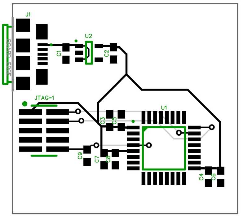
Routing the PCB (black traces on the top layer, gray traces on the bottom layer)
When routing on a PCB you want to minimize the length of each trace as much as possible. You also want to minimize the number of vias and avoid any 90 degree bends in the traces. These recommendations are especially critical for high power traces and high speed signals.
A via is a hole between layers with conducting material that allows you to connect together two traces on different layers. Most vias are what are known as through vias which means the via tunnels through all layers of the board.
Through vias are the simplest type to manufacture because they can be drilled after the entire PCB layer stack-up is assembled.
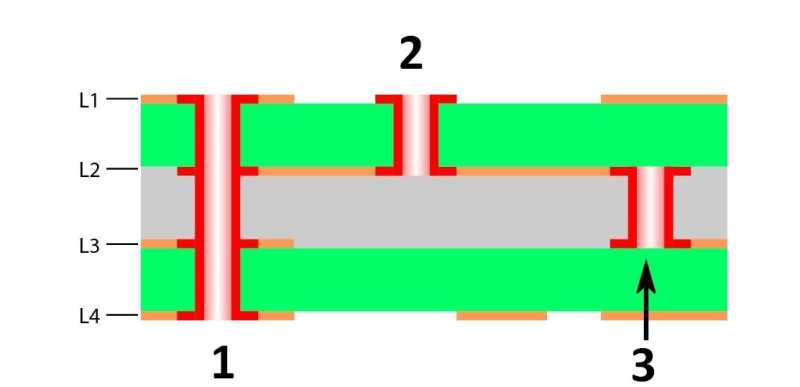
Via #1 is a classic through via, via #2 is a blind via, and via #3 is a buried via.
Vias that only tunnel through a subset of layers are known as buried and blind vias. Blind vias connect an external layer to an internal layer (so one end is hidden inside the PCB stack-up). Buried vias connect two internal layers and are completely hidden on the assembled PCB.
Blind and buried vias allow you to pack a design more tightly. This is because they don’t take up space on the layers not using them. Through vias on the other hand consume space on all layers.
However, be aware that blind and buried vias drastically increase the prototype cost for your board. In most situations you should restrict yourself to only using through vias. Only exceptionally complex designs, that must fit in an exceptionally small space, should likely ever require these more advanced via types.
When routing any high current power lines you need to ensure the trace width is capable of carrying the necessary current. If you run too much current through a PCB trace it will overheat and melt causing the board to become defective.
To determine the necessary trace width I like to use a PCB trace width calculator. To determine the required trace width you need to first know the trace thickness for your specific PCB process.
PCB manufacturers allow you to select various conducting layer thicknesses, usually measured in ounces per square foot (oz/ft2) but also measured in mils (a mil is one thousandth of an inch) or millimeters.
A common conducting layer thickness is 1 oz/ft2. In this tutorial I’ve made the power supply lines 10 mils wide. Using the calculator linked to above shows that a 1 oz/ft2 trace measuring 10 mils wide can actually carry almost 900mA of current.
This is obviously much more than we’ll need, and I could have easily made the supply lines much more narrow. In the first tutorial I showed that the absolute maximum current required by the STM32F042 is 120mA. Perhaps surprisingly, to handle 120mA we only need a trace width of 0.635 mils!
The minimum trace width allowed by most processes is 4-6 mils. The minimum width traces can be easily used for the supply lines in this design. That being said, the wider the trace the less the resistance and the more stable the supply voltage at each component.
Unless space is extremely tight you should always over design the power supply traces. In fact, in many cases you’ll want the power supply routing on its own layer so you can maximize the routing width.
Finally, in the calculator you’ll notice the requirements are different for internal layers versus external layers. For this simple, 2-layer design both layers are external so the “Results for External Layers in Air” is what we need to use.
Internal layers can carry much less current because they don’t get the cooling effect of being exposed to air so the traces will overheat with much less current.
The completed Printed Circuit Board (PCB) layout for this initial tutorial.
Once all of the routing is done it’s time to perform verifications to ensure everything is correct. This is where automation really works well and any PCB design tool will offer automatic verification features.
There are broadly two types of verification: design rules check (DRC) and schematic comparison.
The DRC verifies that all PCB process design rules have been followed. This includes rules such as the minimum allowed trace width, the minimum spacing allowed between traces, the minimum spacing between a trace and the board edge, and so on.
In order to run a DRC verification its necessary that you first obtain all of the design rules for the specific PCB process you will be using.
Each PCB prototyping process has slightly different rules so you must have the correct rules before proceeding. You can get the design rules for your specific process from your PCB prototype supplier.
In DipTrace, you define the design rules by selecting Verification->Design Rules. Once all rules have been correctly defined, you can run the DRC by selecting Verification->Check Design Rules.
After you have verified that your PCB layout adheres to all of the process design rules, it’s now time to verify that your PCB design matches your schematic diagram. To do this in DipTrace you simply select Verification->Compare to Schematic.
In future tutorials, I’ll show you various types of DRC and schematic comparison errors, and how to fix them.
Once you have verified the design adheres to the process design rules and matches the schematic diagram, it’s time to order your PCB prototypes.
In order to do this you’ll need to convert your PCB layout design (which is currently stored in a proprietary file format) into the industry standard file format known as Gerber.
The Gerber format outputs each layer of your PCB design as a separate file. The generated layers are much more than just the conducting layers of your board. Some of those layers include:
1) Silk layers – Includes the text and component designators.
2) Assembly layers – Similar to silk layers but with specific assembly instructions.
3) Solder mask layers – Indicates the green stuff on a PCB that covers up any conductors that you don’t want to solder to. This prevents accidental shorts during soldering.
4) Solder paste layers – Used to precisely place solder paste where soldering will occur.
You will also need to generate what is known as a Pick-and-Place file which includes the coordinates and orientation for all of the components. This file is used by the manufacturer’s automatic component placement machines.
Finally, you need to output a drill file that provides the exact location and size of any holes such as vias and mounting holes.
Once you have the Gerbers, the Pick-and-Place file, and the drill file you can send those files to any prototype shop or manufacturer for production of your board.
In this tutorial you’ve learned how to design a system-level block diagram, select all of the critical components, design the full schematic circuit diagram, design the Printed Circuit Board (PCB) layout, and order prototypes of your completed microcontroller PCB design.
This tutorial has purposefully kept the circuit itself rather simple so as to not overwhelm you with circuit complexity. That being said, a microcontroller without any additional functionality isn’t very useful.
Note: The content and the pictures in this article are contributed by John Teel. This article was originally published at PredictableDesigns.com


